Toggle light / dark theme

Researchers are a step closer to realizing a new kind of memory that works according to the principles of spintronics which is analogous to, but different from, electronics. Their unique gallium arsenide-based ferromagnetic semiconductor can act as memory by quickly switching its magnetic state in the presence of an induced current at low power. Previously, such current-induced magnetization switching was unstable and drew a lot of power, but this new material both suppresses the instability and lowers the power consumption too.

The field of quantum computing often gets covered in the technical press; however, another emerging field along similar lines tends to get overlooked, and that is spintronics. In a nutshell, spintronic devices could replace some and offer greater performance at far low power levels. Electronic devices use the motion of electrons for power and communication. Whereas use a transferable property of stationary electrons, their angular momentum, or spin. It’s a bit like having a line of people pass on a message from one to the other rather than have the person at one end run to the other. Spintronics reduces the effort needed to perform computational or memory functions.

Spintronic-based memory devices are likely to become common as they have a useful feature in that they are nonvolatile, meaning that once they are in a certain state, they maintain that state even without power. Conventional computer memory, such as DRAM and SRAM made of ordinary semiconductors, loses its state when it’s powered off. At the core of experimental spintronic devices are that can be magnetized in opposite directions to represent the familiar binary states of 1 or 0, and this switching of states can occur very, very quickly. However, there has been a long and arduous search for the best materials for this job, as magnetizing spintronic materials are no simple matter.

Researchers identify Brown-Zak fermions in superlattices made from the carbon sheet.


Researchers at the University of Manchester in the UK have identified a new family of quasiparticles in superlattices made from graphene sandwiched between two slabs of boron nitride. The work is important for fundamental studies of condensed-matter physics and could also lead to the development of improved transistors capable of operating at higher frequencies.

In recent years, physicists and materials scientists have been studying ways to use the weak (van der Waals) coupling between atomically thin layers of different crystals to create new materials in which electronic properties can be manipulated without chemical doping. The most famous example is graphene (a sheet of carbon just one atom thick) encapsulated between another 2D material, hexagonal boron nitride (hBN), which has a similar lattice constant. Since both materials also have similar hexagonal structures, regular moiré patterns (or “superlattices”) form when the two lattices are overlaid.

If the stacked layers of graphene-hBN are then twisted, and the angle between the two materials’ lattices decreases, the size of the superlattice increases. This causes electronic band gaps to develop through the formation of additional Bloch bands in the superlattice’s Brillouin zone (a mathematical construct that describes the fundamental ideas of electronic energy bands). In these Bloch bands, electrons move in a periodic electric potential that matches the lattice and do not interact with one another.

Faster, smaller, smarter and more energy-efficient chips for everything from consumer electronics to big data to brain-inspired computing could soon be on the way after engineers at The University of Texas at Austin created the smallest memory device yet. And in the process, they figured out the physics dynamic that unlocks dense memory storage capabilities for these tiny devices.

The research published recently in Nature Nanotechnology builds on a discovery from two years ago, when the researchers created what was then the thinnest storage device. In this new work, the researchers reduced the size even further, shrinking the cross section area down to just a single square nanometer.

Getting a handle on the physics that pack dense memory storage capability into these devices enabled the ability to make them much smaller. Defects, or holes in the material, provide the key to unlocking the high-density memory storage capability.

Scientists at Osaka University develop a label-free method for identifying respiratory viruses based on changes in electrical current when they pass through silicon nanopores, which may lead to new rapid COVID-19 tests.

The ongoing global pandemic has created an urgent need for rapid tests that can diagnose the presence of the SARS-CoV-2 virus, the pathogen that causes COVID-19, and distinguish it from other respiratory viruses. Now, researchers from Japan have demonstrated a new system for single-virion identification of common respiratory pathogens using a machine learning algorithm trained on changes in current across silicon nanopores. This work may lead to fast and accurate screening tests for diseases like COVID-19 and influenza.

In a study published this month in ACS Sensors scientists at Osaka University have introduced a new system using silicon nanopores sensitive enough to detect even a single virus particle when coupled with a machine learning algorithm.

Throughout all known space, between the stars and the galaxies, an extremely faint glow suffuses, a relic left over from the dawn of the Universe. This is the cosmic microwave background (CMB), the first light that could travel through the Universe when it cooled enough around 380,000 years after the Big Bang for ions and electrons to combine into atoms.

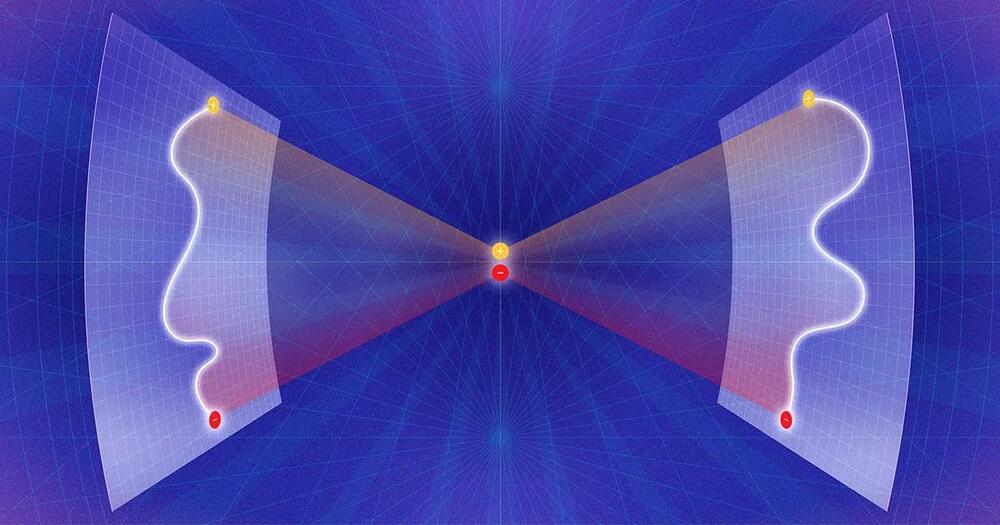
But now scientists have discovered something peculiar about the CMB. A new measurement technique has revealed hints of a twist in the light — something that could be a sign of a violation of parity symmetry, hinting at physics outside the Standard Model.

According to the Standard Model of physics, if we were to flip the Universe as though it were a mirror reflection of itself, the laws of physics should hold firm. Subatomic interactions should occur in exactly the same way in the mirror as they do in the real Universe. This is called parity symmetry.

Researchers have recently displayed the interaction of superconducting qubits; the basic unit of quantum information, with surface acoustic wave resonators; a surface-wave equivalent of the crystal resonator, in quantum physics. This phenomena opens a new field of research, defined as quantum acoustodynamics to allow the development of new types of quantum devices. The main challenge in this venture is to manufacture acoustic resonators in the gigahertz range. In a new report now published on Nature Communications Physics, Aleksey N. Bolgar and a team of physicists in Artificial Quantum Systems and Physics, in Russia and the U.K., detailed the structure of a significantly simplified hybrid acoustodynamic device by replacing an acoustic resonator with a phononic crystal or acoustic metamaterial.

The crystal contained narrow metallic stripes on a quartz surface and this artificial atom or metal object in turn interacted with a microwave transmission line. In engineering, a transmission line is a connector that transmits energy from one point to another. The scientists used the setup to couple two degrees of freedom of different nature, i.e. acoustic and electromagnetic, with a single quantum object. Using a scattering spectrum of propagating electromagnetic waves on the they visualized acoustic modes of the phononic crystal. The geometry of the device allowed them to realize the effects of quantum acoustics on a simple and compact system.

Physicists at the Max Planck Institute of Quantum Optics have tested quantum mechanics to a completely new level of precision using hydrogen spectroscopy, and in doing so they came much closer to solving the well-known proton charge radius puzzle.

Scientists at the Max Planck Institute of Quantum Optics (MPQ) have succeeded in testing quantum electrodynamics with unprecedented accuracy to 13 decimal places. The new measurement is almost twice as accurate as all previous hydrogen measurements combined and moves science one step closer to solving the proton size puzzle. This high accuracy was achieved by the Nobel Prize-winning frequency comb technique, which debuted here for the first time to excite atoms in high-resolution spectroscopy. The results are published today in Science.

Physics is said to be an exact science. This means that predictions of physical theories – exact numbers – can be verified or falsified by experiments. The experiment is the highest judge of any theory. Quantum electrodynamics, the relativistic version of quantum mechanics, is without doubt the most successful theory to date. It allows extremely precise calculations to be performed, for example, the description of the spectrum of atomic hydrogen to 12 decimal places. Hydrogen is the most common element in the universe and at the same time the simplest with only one electron. And still, it hosts a mystery yet unknown.

Physicists use a Bose-Einstein condensate to study phase transitions in an iron pnictide superconductor.


Physicists have deployed a Bose-Einstein condensate (BEC) as a “quantum microscope” to study phase transitions in a high-temperature superconductor. The experiment marks the first time a BEC has been used to probe such a complicated condensed-matter phenomenon, and the results – a solution to a puzzle involving transition temperatures in iron pnictide superconductors – suggest that the technique could help untangle the complex factors that enhance and inhibit high-temperature superconductivity.

A BEC is a state of matter that forms when a gas of bosons (particles with integer quantum spin) is cooled to such low temperatures that all the bosons fall into the same quantum state. Under these conditions, the bosons are highly sensitive to tiny fluctuations in the local magnetic field, which perturb their collective wavefunction and create patches of greater and lesser density in the gas. These variations in density can then be detected using optical techniques.

The new instrument, known as a scanning quantum cryogenic atom microscope (SQCRAMscope), puts this magnetic field sensitivity to practical use. “Our SQCRAMscope is basically like a microscope – a big lens, focusing light down on a sample, looking at the reflected light – except right at the focus we have a collection of quantum atoms that transduces the magnetic field into a light field,” explains team leader Benjamin Lev, a physicist at Stanford University in the US. “It’s a quantum gas transducer.”

The discovery “reinforces our confidence that we understand how stars work.”


New Life

Scientists had already found neutrinos given off when the Sun fuses hydrogen into helium, a hallmark process of lighter stars that gives off 99 percent of the sun’s energy. The new discovery not only extended the lifespan of the Borexino detector — which was scheduled to be decommissioned next month — but also revitalized scientists’ understanding of the cosmos.

“Confirmation of CNO burning in our sun, where it operates at only one percent, reinforces our confidence that we understand how stars work,” UMass Amherst physicist Andrea Pocar said in the release.

Neutrinos Yield First Experimental Evidence of Catalyzed Fusion Dominant in Many Stars

An international team of about 100 scientists of the Borexino Collaboration, including particle physicist Andrea Pocar at the University of Massachusetts Amherst, report in Nature this week detection of neutrinos from the sun, directly revealing for the first time that the carbon-nitrogen-oxygen (CNO) fusion-cycle is at work in our sun.

The CNO cycle is the dominant energy source powering stars heavier than the sun, but it had so far never been directly detected in any star, Pocar explains.