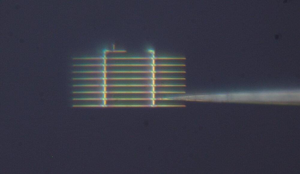
Menu

Blog

Archive for the ‘particle physics’ category: Page 351

Aug 13, 2020

Engineers manipulate color on the nanoscale, making it disappear

Posted by in categories: chemistry, nanotechnology, particle physics

Most of the time, a material’s color stems from its chemical properties. Different atoms and molecules absorb different wavelengths of light; the remaining wavelengths are the “intrinsic colors” that we perceive when they are reflected back to our eyes.

So-called “” works differently; it’s a property of physics, not chemistry. Microscopic patterns on some surfaces reflect light in such a way that different wavelengths collide and interfere with one another. For example, a peacock’s feathers are made of transparent protein fibers that have no intrinsic color themselves, yet we see shifting, iridescent blue, green and purple hues because of the nanoscale structures on their surfaces.

As we become more adept at manipulating structure at the smallest scales, however, these two types of color can combine in even more surprising ways. Penn Engineers have now developed a system of nanoscale semiconductor strips that uses structural color interactions to eliminate the strips’ intrinsic color entirely.

Aug 12, 2020

Physicists accelerate the hunt for revolutionary artificial atomic materials

Posted by in categories: materials, particle physics

Scientists at the University of Bath have taken an important step towards understanding the interaction between layers of atomically thin materials arranged in stacks. They hope their research will speed up the discovery of new, artificial materials, leading to the design of electronic components that are far tinier and more efficient than anything known today.

Smaller is always better in the world of electronic circuitry, but there’s a limit to how far you can shrink a silicon component without it overheating and falling apart, and we’re close to reaching it. The researchers are investigating a group of atomically thin materials that can be assembled into stacks. The properties of any final material depend both on the choice of raw materials and on the angle at which one layer is arranged on top of another.

Dr. Marcin Mucha-Kruczynski who led the research from the Department of Physics, said: “We’ve found a way to determine how strongly atoms in different layers of a stack are coupled to each other, and we’ve demonstrated the application of our idea to a structure made of .”

Aug 8, 2020

Microplastics have moved into virtually every crevice on Earth

Posted by in categories: nanotechnology, particle physics

O,.o Maybe nanomagnets could essentially collect these particles in the future or an enzyme could be introduced.


A collection of new research provides more clues about where and how microplastics are spreading.

Aug 8, 2020

Tiniest secrets of integrated circuits revealed with new imaging technique

Posted by in categories: computing, particle physics, quantum physics

The life-givers of integrated circuits and quantum devices in silicon are small structures made from patches of foreign atoms called dopants. The dopant structures provide charge carriers that flow through the components of the circuit, giving the components their ability to function. These days the dopant structures are only a few atoms across and so need to be made in precise locations within a circuit and have very well-defined electrical properties. At present manufacturers find it hard to tell in a non-destructive way whether they have made their devices according to these strict requirements. A new imaging paradigm promises to change all that.

The imaging mode called broadband electric force microscopy, developed by Dr. Georg Gramse at Keysight technologies & JKU uses a very sharp probe that sends into a silicon chip, to image and localize structures underneath the surface. Dr. Gramse says that because the microscope can use waves with many frequencies it can provide a wealth of previously inaccessible detail about the electrical environment around the dopant structures. The extra information is crucial to predicting how well the devices will ultimately perform.

The imaging approach was tested on two tiny dopant structures made with a templating process which is unique in achieving atomically sharp interfaces between differently doped regions. Dr. Tomas Skeren at IBM produced the world’s first electronic diode (a circuit component which passes current in only one direction) fabricated with this templating process, while Dr. Alex Kölker at UCL created a multilevel 3D with atomic scale precision.

Aug 7, 2020

Physicists watch quantum particles tunnel through solid barriers. Here’s what they found

Posted by in categories: particle physics, quantum physics

A team of physicists has devised a simple way to measure the duration of a bizarre phenomenon called quantum tunneling.

Aug 7, 2020

An electrical switch for magnetism

Posted by in categories: computing, nanotechnology, particle physics

NUS physicists have demonstrated the control of magnetism in a magnetic semiconductor via electrical means, paving the way for novel spintronic devices.

Semiconductors are the heart of information-processing technologies. In the form of a transistor, semiconductors act as a switch for , allowing switching between binary states zero and one. Magnetic materials, on the other hand, are an essential component for information storage devices. They exploit the spin degree of freedom of electrons to achieve memory functions. Magnetic semiconductors are a unique class of materials that allow control of both the electrical charge and spin, potentially enabling information processing and memory operations in a single platform. The key challenge is to control the electron spins, or magnetisation, using electric fields, in a similar way a transistor controls electrical charge. However, magnetism typically has weak dependence on electric fields in magnetic semiconductors, and the effect is often limited to .

A research team led by Prof Goki EDA from the Department of Physics and the Department of Chemistry, and the Centre for Advanced 2-D Materials, NUS, in collaboration with Prof Hidekazu KUREBAYASHI from the London Centre for Nanotechnology, University College London, discovered that the magnetism of a magnetic semiconductor, Cr2Ge2Te6, shows exceptionally strong response to applied electric fields. With electric fields applied, the material was found to exhibit ferromagnetism (a state in which electron spins spontaneously align) at temperatures up to 200 K (−73°C). At such temperatures, ferromagnetic order is normally absent in this material.

Aug 7, 2020

Researchers show how to make non-magnetic materials magnetic

Posted by in categories: computing, particle physics

O,.o well then anything could be a computer even a mushroom or a rock :3.


A complex process can modify non-magnetic oxide materials in such a way to make them magnetic. The basis for this new phenomenon is controlled layer-by-layer growth of each material. An international research team with researchers from Martin Luther University Halle-Wittenberg (MLU) reported on their unexpected findings in the journal Nature Communications.

In solid-state physics, oxide layers only a few nanometres thick are known to form a so-called two-dimensional electron gas. These thin layers, separated from one another, are transparent and electrically insulating materials. However, when one grows on top of the other, a conductive area forms under certain conditions at the interface, which has a metallic shine. “Normally this system remains non-magnetic,” says Professor Ingrid Mertig from the Institute of Physics at MLU. The research team has succeeded in controlling conditions during growth so that vacancies are created in the atomic layers near the interface. These are later filled in by other atoms from adjoining atomic layers.

Continue reading “Researchers show how to make non-magnetic materials magnetic” »

Aug 6, 2020

After nearly a century, elusive CNO neutrinos are finally seen from the Sun

Posted by in category: particle physics

For the first time, scientists have detected neutrinos coming from the Sun’s core that got their start via the CNO process, an until-now theorized type of stellar nuclear fusion.

This is really cool, but it’ll take a bit of explaining.

Aug 6, 2020

Spacecraft of the Future Could Be Powered By Lattice Confinement Fusion

Posted by in categories: particle physics, space travel

NASA researchers demonstrate the ability to fuse atoms inside room-temperature metals.

Aug 5, 2020

W and Z particles discovered

Posted by in category: particle physics

In 1979, CERN decided to convert the Super Proton Synchrotron (SPS) into a proton–antiproton collider. A technique called stochastic cooling was vital to the project’s success as it allowed enough antiprotons to be collected to make a beam.

The first proton–antiproton collisions were achieved just two years after the project was approved, and two experiments, UA1 and UA2, started to search the collision debris for signs of W and Z particles, carriers of the weak interaction between particles.

In 1983, CERN announced the discovery of the W and Z particles. The image above shows the first detection of a Z0 particle, as seen by the UA1 experiment on 30 April 1983. The Z0 itself decays very quickly so cannot be seen, but an electron–positron pair produced in the decay appear in blue. UA1 observed proton-antiproton collisions on the SPS between 1981 and 1993 to look for the Z and W bosons, which mediate the weak fundamental force.