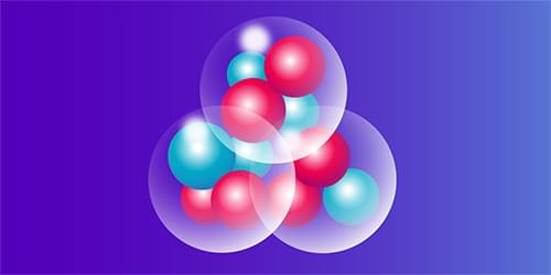
When two helium-4 (4He) nuclei smash together, they form a beryllium-8 nucleus. A third 4 He striking this nucleus may result in an excited form of carbon-12 (12 C), with the 4 He particles arranging in a neat cluster. Clustering of neutrons and protons during high-energy collisions is known to determine the stability of the collision products. But how clustering affects the dynamics and reaction outcomes of high-energy collisions remains an open question. Now Catalin Frosin of the University of Florence, Italy, and his colleagues report experimental data that detail how reaction products form during this kind of collision [1]. The results support models that suggest increased collision energy can drive clustering activity and result in emission of lighter, more energetic particles.
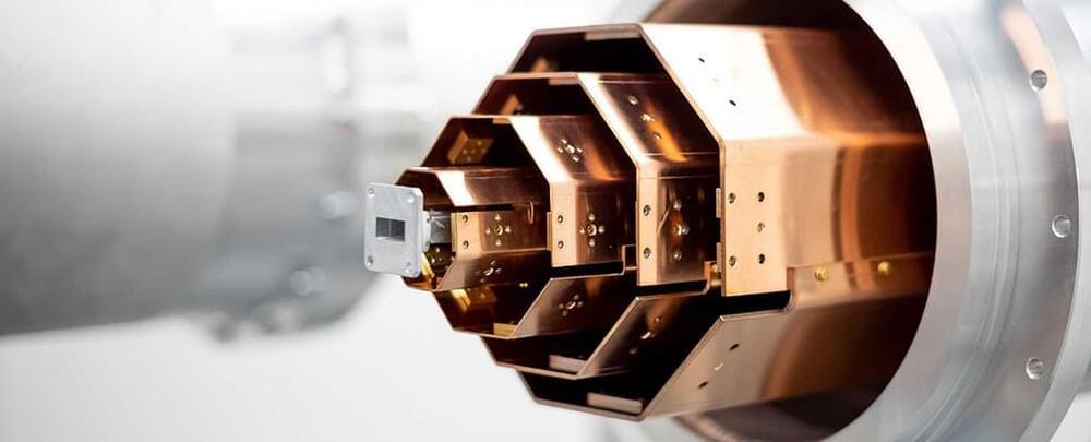
The experiments entail bombarding 12 C targets with pulsed beams of sulfur-32 and neon-20. Frosin and his colleagues characterized the resulting fragments using FAZIA, a detector designed to probe charged particles around the Fermi energy. Meanwhile, the team ran simulations, with and without cluster correlations, to predict the nucleon interactions and the decays of unstable products. Models with clustering produced particles that are more energetic—in agreement with the experimental data. The researchers attributed this effect to energy and momentum conservation in the nucleon–nucleon and nucleon–cluster collisions during the early, dynamic phase of the interaction.
The findings demonstrate FAZIA’s capability to extract precise information about the properties of nuclear fragments. The researchers say that similar experiments performed elsewhere looked only at carbon+carbon reactions. Extending them to heavier reactants provides a wider arena for interpreting fragmentation mechanisms.