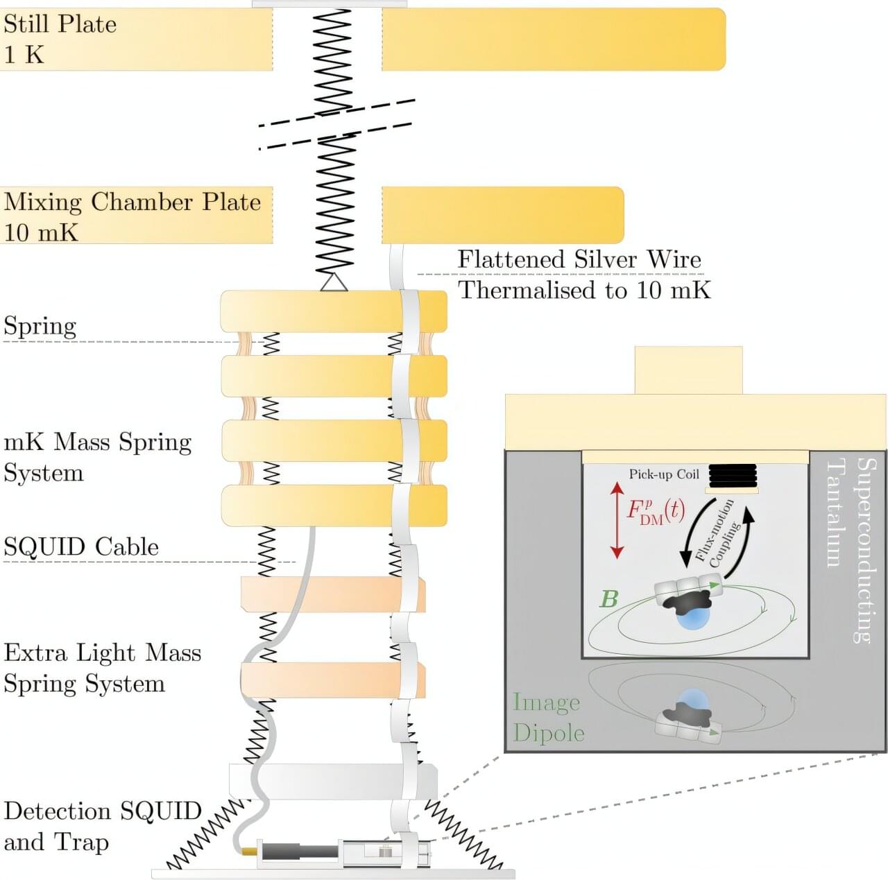
Toggle light / dark theme

Sept 22 2016.


Kurzweilai – How the properties of quarks and gluons can be used (in principle) to perform computation at the femtometer (10^−15 meter) scale.

An atom is about 10^−10 m in size.

The next smallest thing in nature is the nucleus, which is about 100,000 times smaller, i.e., 10^−15 m in size — a femtometer, or “fermi.” A nucleus is composed of protons and neutrons (i.e., “nucleons”), which we now know are composed of 3 quarks, which are bound (“glued”) together by massless (photon-like) particles called “gluons.”

The U.S. Naval Research Laboratory (NRL), in collaboration with Kansas State University, has discovered slab waveguides based on the two-dimensional material hexagonal boron nitride. This milestone has been reported in the journal Advanced Materials.

Two-dimensional (2D) materials are a class of materials that can be reduced to the monolayer limit by mechanically peeling the layers apart. The weak interlayer attractions (van der Waals attraction) allow the layers to be separated via the so-called “Scotch tape” method.

The most well-known 2D material, graphene, is a semimetallic material consisting of a single layer of carbon atoms. Recently, other 2D materials including semiconducting (TMDs) and insulating hexagonal boron nitride (hBN) have also garnered attention. When reduced near the monolayer limit, 2D materials have unique nanoscale properties that are appealing for creating atomically thin electronic and .

Infleqtion is unique amongst quantum companies due its participation in so many different segments of the quantum computing industry including quantum components, quantum computers, quantum software, and quantum sensors. This strategy of a broad product portfolio provides both advantages and disadvantages for a company. The potential advantages include achieving synergy between different product areas with the neutral atom, atomic prism, photonic, software, and other technologies they have developed over the years. It also brings some diversity in the revenue streams because some products will provide early revenue while others might take a few years of development before they can make a revenue contribution. The potential disadvantages could include execution risks if the engineering resources are spread too thin. Also, there may be different sets of customers and sales channels for the different product lines which can increase the complexities of managing a sales force, calling on customers, and generating new business.

Nonetheless, Infleqtion has made some interesting announcements in the past few months. In 2023 alone, the Quantum Computing Report by GQI ran 17 different stories that included Infleqtion. This week they hosted a webinar to discuss their product roadmaps for sensors, software, and computing. The highlight of the webinar was the announcement of their quantum computing roadmap. In this article, we will cover their plans for quantum computing, but first we will start with the progress they talked about in quantum sensors and quantum software and then discuss quantum computing afterwards.

Infleqtion’s discussion of sensor products included ones named Tiqker, Sqywire, and eXaqt. Tiqker is a small form factor ultra-accurate clock intended for use in navigation, data centers, and communication networks. The company asserts that this clock is 100X more accurate than cesium beam atomic clocks and 100,000X more accurate than a crystal oscillator. In navigation applications it can be used in GPS-denied environments and in communication networks it can help increase bandwidth and reduce latencies due to the more precise clocking of the data signals. The company mentioned that they are partnering with a large company for use of Tiqker in data center applications and that Tiqker is now available for pre-order. Sqywire is an ultra-sensitive radio frequency (RF) receiver that senses RF signals with Rydberg state atom-based sensing. It can be used installed of a classical antenna and provides high sensitivity, lower power, and ultra-wide bandwidth in a form factor.

Neutron stars in the universe, ultracold atomic gases in the laboratory, and the quark–gluon plasma created in collisions of atomic nuclei at the Large Hadron Collider (LHC): they may seem totally unrelated but, surprisingly enough, they have something in common. They are all a fluid-like state of matter made up of strongly interacting particles. Insights into the properties and behavior of any of these almost-perfect liquids may be key to understanding nature across scales that are orders of magnitude apart.

In a new paper, the CMS collaboration reports the most precise measurement to date of the speed at which sound travels in the quark–gluon plasma, offering new insights into this extremely hot state of matter.

Sound is a longitudinal wave that travels through a medium, producing compressions and rarefactions of matter in the same direction as its movement. The speed of sound depends on the medium’s properties, such as its density and viscosity. It can, therefore, be used as a probe of the medium.

The color centers of diamond are the focus of an increasing number of research studies, due to their potential for developing quantum technologies. Some works have particularly explored the use of negatively-charged group-IV diamond defects, which exhibit an efficient spin-photon interface, as the nodes of quantum networks.

Researchers at Ulm University in Germany recently leveraged a Germanium vacancy (GeV) center in diamond to realize a . The resulting quantum memory, presented in a Physical Review Letters paper, was found to exhibit a promising coherence time of more than 20 ms.

“Our research group’s primary focus is the exploration of diamond color centers for quantum applications,” Katharina Senkalla, co-author of the paper, told Phys.org. “The most popular defect of diamond so far has been the nitrogen-vacancy center, but, recently, other color centers have also become a focus of research. These consist of an element from the IV column of the periodic table—Si, Ge, Sn or Pb, and a lattice vacancy (i.e., missing next-neighbor carbon atom).”

Recent research has broken the size limitation of traditional ferroelectric effects, providing experimental evidence and theoretical simulations to confirm that a structure with as few as 5,000 atoms can still exhibit solid-state ferroelectric effects.

The studies, by a joint team from Israel and China, are published in Nature Electronics and Nature Communications under the titles “Ferroelectricity in zero-dimensional” and “0D van der Waals interfacial sliding Ferroelectricity,” respectively.

The ferroelectric effect is a physical phenomenon discovered in the early 20th century by Joseph Valasek, and it provides an important technological route for achieving information storage. Traditional ferroelectric effects are subject to size limitations.

In an experiment akin to stop-motion photography, scientists have isolated the energetic movement of an electron while “freezing” the motion of the much larger atom it orbits in a sample of liquid water.

The findings, reported in the journal Science, provide a new window into the electronic structure of molecules in the liquid phase on a timescale previously unattainable with X-rays. The new technique reveals the immediate electronic response when a target is hit with an X-ray, an important step in understanding the effects of radiation exposure on objects and people.

“The induced by radiation that we want to study are the result of the electronic response of the target that happens on the timescale,” said Linda Young, a senior author of the research and Distinguished Fellow at Argonne National Laboratory.

Auger electron spectroscopy (AES) is an incredibly useful technique for probing material samples—but current assumptions about the process ignore some of the key time-dependent effects it involves. So far, this has resulted in overly-simplified calculations, which have ultimately prevented the technique from reaching its full potential.

In a study published in The European Physical Journal Plus Alberto Noccera at the University of British Columbia, Canada, together with Adrian Feiguin at Northeastern University, United States, developed a which offers a more precise theoretical description of the AES process, while taking its time dependence into account. Their method could help researchers to improve their quality of material analysis across a wide array of fields: including chemistry, , and microelectronics.

In the Auger process, an inner-shell electron is initially kicked out of its atom, often through an impact with an energetic light pulse. Afterward, the vacancy it leaves behind is filled by an outer-shell electron.

The proton, that little positively-charged nugget inside an atom, is fractions of a quadrillionth of a meter smaller than anyone thought, according to new research appearing Nov. 7 in Nature.

In work they hope solves the contentious “proton radius puzzle” that has been roiling some corners of physics in the last decade, a team of scientists including Duke physicist Haiyan Gao have addressed the question of the proton’s radius in a new way and discovered that it is 0.831 femtometers across, which is about 4 percent smaller than the best previous measurement using electrons from accelerators. (Read the paper!)

A single femtometer is 0.000000000000039370 inches imperial, if that helps, or think of it as a millionth part of a billionth part of a meter. And the new radius is just 80 percent of that.

Futuristic advancements in AI and healthcare stole the limelight at the tech extravaganza Consumer Electronics Show (CES) 2024. However, battery technology is the game-changer at the heart of these innovations, enabling greater power efficiency. Importantly, electric vehicles are where this technology is being applied most intensely. Today’s EVs can travel around 700km on a single charge, while researchers are aiming for a 1,000km battery range. Researchers are fervently exploring the use of silicon, known for its high storage capacity, as the anode material in lithium-ion batteries for EVs. However, despite its potential, bringing silicon into practical use remains a puzzle that researchers are still working hard to piece together.

Enter Professor Soojin Park, PhD candidate Minjun Je, and Dr. Hye Bin Son from the Department of Chemistry at Pohang University of Science and Technology (POSTECH). They have cracked the code, developing a pocket-friendly and rock-solid next-generation high-energy-density Li-ion battery system using micro silicon particles and gel polymer electrolytes. This work was published on the online pages of Advanced Science on the 17th of January.

Employing silicon as a battery material presents challenges: It expands by more than three times during charging and then contracts back to its original size while discharging, significantly impacting battery efficiency. Utilizing nano-sized silicon (10-9m) partially addresses the issue, but the sophisticated production process is complex and astronomically expensive, making it a challenging budget proposition. By contrast, micro-sized silicon (10-6m) is superbly practical in terms of cost and energy density. Yet, the expansion issue of the larger silicon particles becomes more pronounced during battery operation, posing limitations for its use as an anode material.