Toggle light / dark theme

Scientists from the Friedrich Schiller University Jena and the Friedrich Alexander University Erlangen-Nuremberg, both Germany, have successfully developed nanomaterials using a so-called bottom-up approach. As reported in the journal ACS Nano, they exploit the fact that crystals often grow in a specific direction during crystallization. These resulting nanostructures could be used in various technological applications.

“Our structures could be described as worm-like rods with decorations,” explains Prof. Felix Schacher. “Embedded in these rods are ; in our case, this was silica. However, instead of silica, conductive nanoparticles or semiconductors could also be used—or even mixtures, which can be selectively distributed in the nanocrystals using our method,” he adds. Accordingly, the range of possible applications in science and technology is broad, spanning from information processing to catalysis.

“The primary focus of this work was to understand the preparation method as such,” explains the chemist. To produce nanostructures, he elaborates, there are two different approaches: larger particles are ground down to nanometer size, or the structures are built up from smaller components.

There is a largely untapped energy source along the world’s coastlines: the difference in salinity between seawater and freshwater. A new nanodevice can harness this difference to generate power.

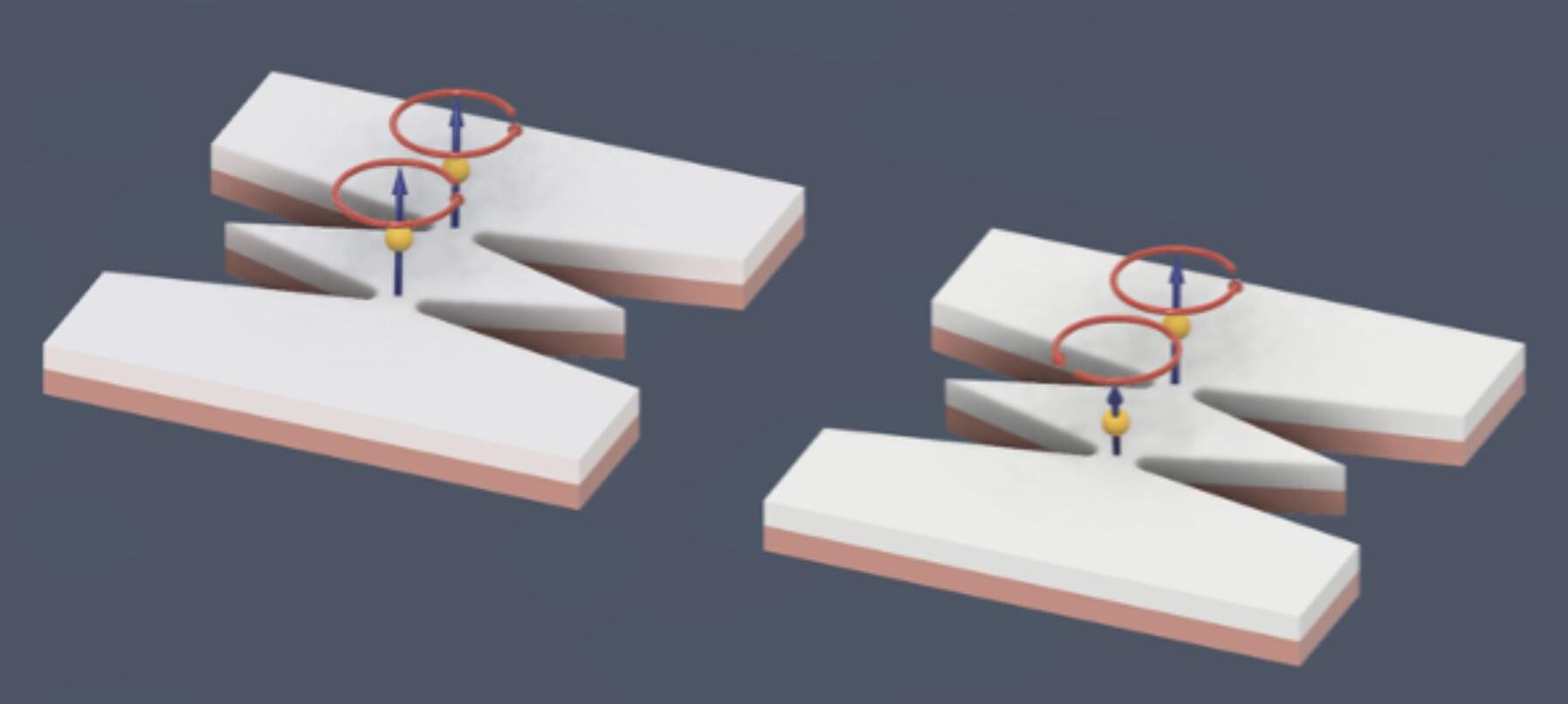
A team of researchers at the University of Illinois Urbana-Champaign has reported a design for a nanofluidic device capable of converting ionic flow into usable electric power in the journal Nano Energy. The team believes that their device could be used to extract power from the natural ionic flows at seawater-freshwater boundaries.

“While our design is still a concept at this stage, it is quite versatile and already shows strong potential for energy applications,” said Jean-Pierre Leburton, a U. of I. professor of electrical & computer engineering and the project lead. “It began with an academic question—’Can a nanoscale solid-state device extract energy from ionic flow?’—but our design exceeded our expectations and surprised us in many ways.”

It lets researchers extract pixel-by-pixel information from nanoscale.

The nanoscale refers to a length scale that is extremely small, typically on the order of nanometers (nm), which is one billionth of a meter. At this scale, materials and systems exhibit unique properties and behaviors that are different from those observed at larger length scales. The prefix “nano-” is derived from the Greek word “nanos,” which means “dwarf” or “very small.” Nanoscale phenomena are relevant to many fields, including materials science, chemistry, biology, and physics.

While the nanobio interaction is crucial in determining nanoparticles’ in vivo fate, a previous work on investigating nanoparticles’ interaction with biological barriers is mainly carried out in a static state. Nanoparticles’ fluid dynamics that share non-negligible impacts on their frequency of encountering biological hosts, however, is seldom given attention. Herein, inspired by badmintons’ unique aerodynamics, badminton architecture Fe3O4&mPDA (Fe3O4 = magnetite nanoparticle and mPDA = mesoporous polydopamine) Janus nanoparticles have successfully been synthesized based on a steric-induced anisotropic assembly strategy. Due to the “head” Fe3O4 having much larger density than the mPDA “cone”, it shows an asymmetric mass distribution, analogous to real badminton.

X-ray free-electron lasers (XFELs) first came into existence two decades ago. They have since enabled pioneering experiments that “see” both the ultrafast and the ultrasmall. Existing devices typically generate short and intense x-ray pulses at a rate of around 100 x-ray pulses per second. But one of these facilities, the Linac Coherent Light Source (LCLS) at the SLAC National Accelerator Laboratory in California, is set to eclipse this pulse rate. The LCLS Collaboration has now announced “first light” for its upgraded machine, LCLS-II. When it is fully up and running, LCLS-II is expected to fire one million pulses per second, making it the world’s most powerful x-ray laser.

The LCLS-II upgrade signifies a quantum leap in the machine’s potential for discovery, says Robert Schoenlein, the LCLS’s deputy director for science. Now, rather than “demonstration” experiments on simple, model systems, scientists will be able to explore complex, real-world systems, he adds. For example, experimenters could peer into biological systems at ambient temperatures and physiological conditions, study photochemical systems and catalysts under the conditions in which they operate, and monitor nanoscale fluctuations of the electronic and magnetic correlations thought to govern the behavior of quantum materials.

The XFEL was first proposed in 1992 to tackle the challenge of building an x-ray laser. Conventional laser schemes excite large numbers of atoms into states from which they emit light. But excited states with energies corresponding to x-ray wavelengths are too short-lived to build up a sizeable excited-state population. XFELs instead rely on electrons traveling at relativistic speed through a periodic magnetic array called an undulator. Moving in a bunch, the electrons wiggle through the undulator, emitting x-ray radiation that interacts multiple times with the bunch and becomes amplified. The result is a bright x-ray beam with laser coherence.

Researchers at MESA+ Institute for Nanotechnology developed a tool that can measure the size of a plasma source and the color of the light it emits simultaneously. “Measuring both at the same time enables us to further improve lithography machines for smaller, faster and improved chips.” The article is highlighted as an Editor’s pick in Optics Letters.

Lithography machines are central to the process of making the microchips that are needed for almost all our . To produce the smallest chips, these machines need precision-engineered lenses, mirrors and light sources. “Traditionally, we could only look at the amount of light produced, but to further improve the chipmaking process, we also want to study the colors of that light and the size of its source,” explains Muharrem Bayraktar, assistant professor at the XUV Optics Group.

The extreme ultraviolet light is emitted by a plasma source, produced by aiming lasers at metal droplets. With sets of special mirrors, this light is aimed at a silicon wafer to create the smallest microchips imaginable. “We want to make the plasma as small as possible. Too large and you ‘waste’ a lot of light because the mirrors cannot catch all the light,” says Bayraktar.