The Buccino Leadership Institute presents Ideas & Trends (2024) Nanotechnology: The Three Lenses — Past, Present and Future.
Category: nanotechnology – Page 74

Study reveals how a sugar-sensing protein acts as a ‘machine’ to switch plant growth—and oil production—on and off
Proteins are molecular machines, with flexible pieces and moving parts. Understanding how these parts move helps scientists unravel the function a protein plays in living things—and potentially how to change its effects. Biochemists at the U.S. Department of Energy’s (DOE) Brookhaven National Laboratory and colleagues at DOE’s Pacific Northwest National Laboratory (PNNL) have published a new example of how one such molecular machine works.


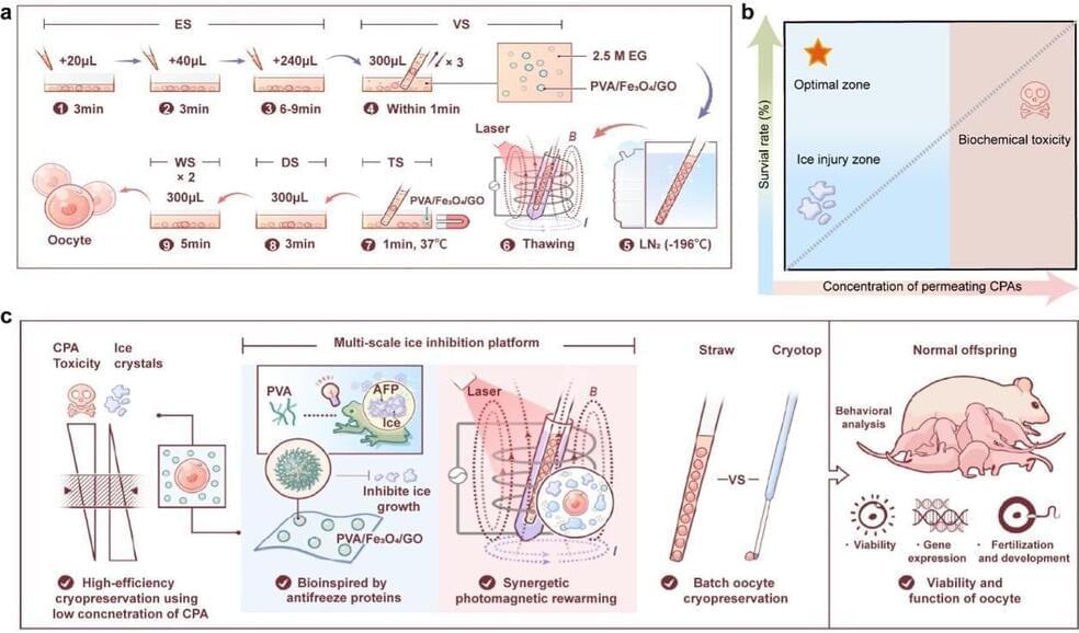
Multi-scale, nanomaterial-based ice inhibition platform enables full-cycle cryogenic protection for mouse oocytes
Safe and high-quality fertility preservation is of growing significance for women in clinical trials. Current primary methods for cryopreserving human oocytes are slow freezing and vitrification, but existing techniques pose risks of biochemical toxicity and are restricted in large-scale clinical practice.
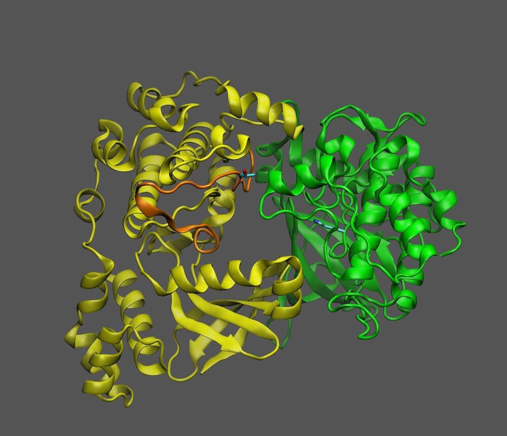
Bionanomachine Breakthrough: A Master Key for Sustainable Chemistry
Scientists at the Paul Scherrer Institute (PSI) have for the first time precisely characterized the enzyme styrene oxide isomerase, which can be used to produce valuable chemicals and drug precursors in an environmentally friendly manner. The study appears today in the journal Nature Chemistry.
Enzymes are powerful biomolecules that can be used to produce many substances at ambient conditions. They enable “green” chemistry, which reduces environmental pollution resulting from processes used in synthetic chemistry. One such tool from nature has now been characterized in detail by PSI researchers: the enzyme styrene oxide isomerase. It is the biological version of the Meinwald reaction, an important chemical reaction in organic chemistry.
“The enzyme, discovered decades ago, is made by bacteria,” says Richard Kammerer of PSI’s Biomolecular Research Laboratory. His colleague Xiaodan Li adds: “But because the way it functions was not known, its practical application has been limited up to now.” The two researchers and their team have elucidated the structure of the enzyme as well as the way it works.
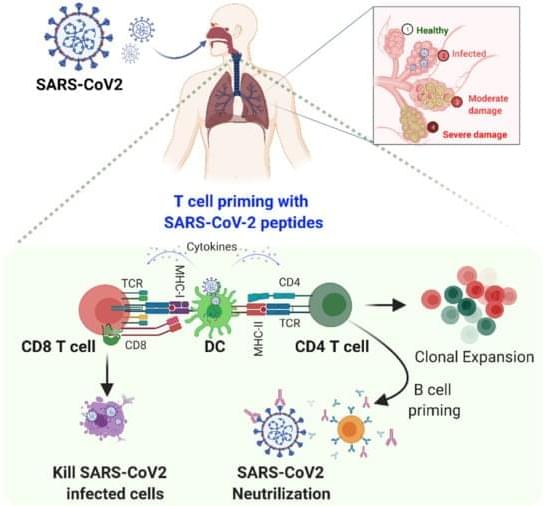
Nanotechnology as a Shield against COVID-19: Current Advancement and Limitations
The coronavirus disease 2019 (COVID-19) caused by severe acute respiratory syndrome coronavirus 2 (SARS-CoV-2) is a global health problem that the WHO declared a pandemic. COVID-19 has resulted in a worldwide lockdown and threatened to topple the global economy. The mortality of COVID-19 is comparatively low compared with previous SARS outbreaks, but the rate of spread of the disease and its morbidity is alarming. This virus can be transmitted human-to-human through droplets and close contact, and people of all ages are susceptible to this virus. With the advancements in nanotechnology, their remarkable properties, including their ability to amplify signal, can be used for the development of nanobiosensors and nanoimaging techniques that can be used for early-stage detection along with other diagnostic tools.