A new nanostructure acts like a wire and switch that can, for the first time, control and direct the flow of quantum quasiparticles called excitons at room temperature.
The transistor-like switch developed by University of Michigan engineers could speed up information transfer or even enable circuits that run on excitons instead of electricity—paving the way for a new class of devices.
Because they have no electrical charge, excitons have the potential to move quantum information without the losses that come with moving electrically charged particles like electrons. These losses drive cell phones and computers to generate heat during use.
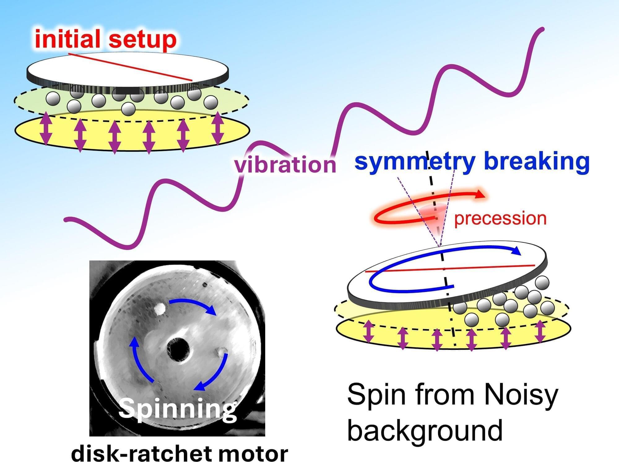
Vibrations are everywhere—from the hum of machinery to the rumble of transport systems. Usually, these random motions are wasted and dissipated without producing any usable work.
Recently, scientists have been fascinated by “ratchet systems,” which are mechanical systems that rectify chaotic vibrations into directional motion. In biology, molecular motors achieve this feat within living cells to drive the essential processes by converting random molecular collisions into purposeful motions. However, at a large scale, these ratchet systems have always relied on built-in asymmetry, such as gears or uneven surfaces.
Moving beyond this reliance on asymmetry, a team of researchers led by Ms. Miku Hatatani, a Ph.D. student at the Graduate School of Science and Engineering, along with Mr. Junpei Oguni, graduate school alumnus at the Graduate School of Science and Engineering, Professor Daigo Yamamoto and Professor Akihisa Shioi from the Department of Chemical Engineering and Materials Science at Doshisha University, demonstrate the world’s first symmetric ratchet motor.
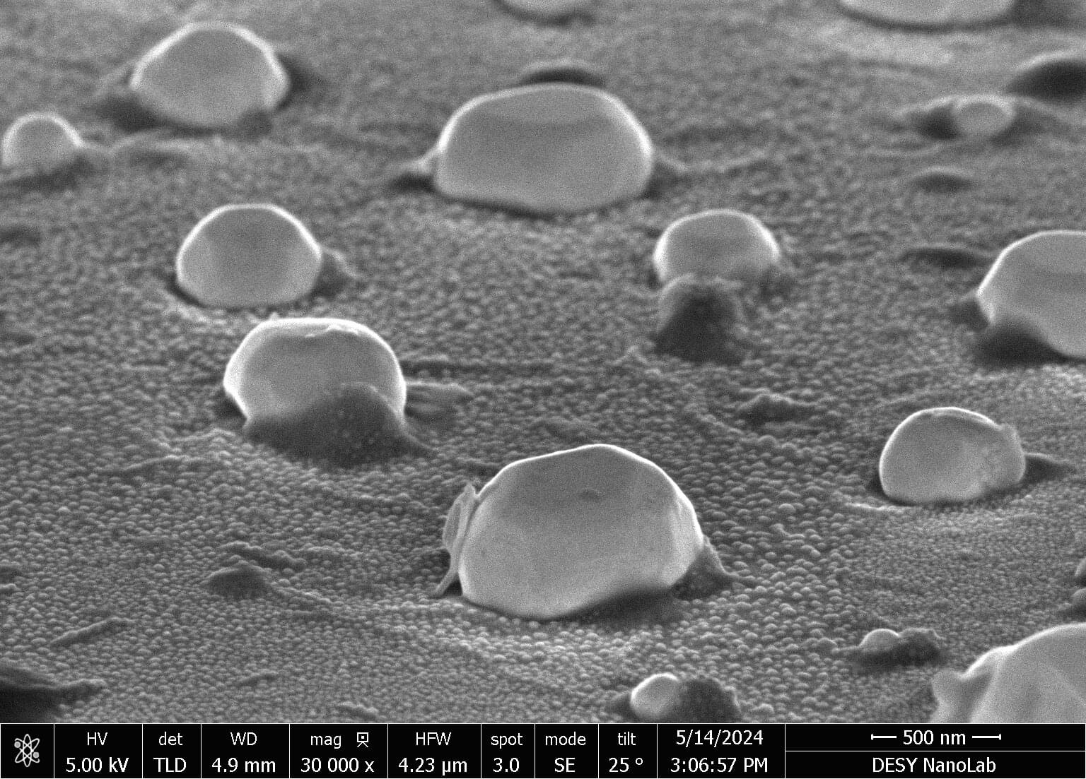
Using a combination of spectromicroscopy at BESSY II and microscopic analyses at DESY’s NanoLab, a team has gained new insights into the chemical behavior of nanocatalysts during catalysis.
The research is published in the journal ACS Nano.
The nanoparticles consisted of a platinum core with a rhodium shell. This configuration allows a better understanding of structural changes in, for example, rhodium– platinum catalysts for emission control. The results show that under typical catalytic conditions, some of the rhodium in the shell can diffuse into the interior of the nanoparticles. However, most of it remains on the surface and oxidizes. This process is strongly dependent on the surface orientation of the nanoparticle facets.
For the protein qubit to “encode” more information about what is going on inside a cell, the fluorescent protein needs to be genetically engineered to match the protein scientists want to observe in a given cell. The glowing protein is then attached to the target protein and zapped with a laser so it reaches a state of superposition, turning it into a nano-probe that picks up what is happening in the cell. From there, scientists can infer how a certain biological process happens, what the beginnings of a genetic disease look like, or how cells respond to certain treatments.
And eventually, this kind of sensing could be used in non-biological applications as well.
“Directed evolution on our EYFP qubit could be used to optimize its optical and spin properties and even reveal unexpected insights into qubit physics,” the researchers said. “Protein-based qubits are positioned to take advantage of techniques from both quantum information sciences and bioengineering, with potentially transformative possibilities in both fields.”
EVANSTON, IL. — With the power to rewrite the genetic code underlying countless diseases, CRISPR holds immense promise to revolutionize medicine. But until scientists can deliver its gene-editing machinery safely and efficiently into relevant cells and tissues, that promise will remain out of reach.
Now, Northwestern University chemists have unveiled a new type of nanostructure that dramatically improves CRISPR delivery and potentially extends its scope of utility.
Called lipid nanoparticle spherical nucleic acids (LNP-SNAs), these tiny structures carry the full set of CRISPR editing tools — Cas9 enzymes, guide RNA and a DNA repair template — wrapped in a dense, protective shell of DNA. Not only does this DNA coating shield its cargo, but it also dictates which organs and tissues the LNP-SNAs travel to and makes it easier for them to enter cells.
New system delivers CRISPR machinery more safely and effectively into cells.
Quantum mechanics theory predicts that, in addition to exhibiting particle-like behavior, particles of all sizes can also have wave-like properties. These properties can be represented using the wave function, a mathematical description of quantum systems that delineates a particle’s movements and the probability that it is in a specific position.
Researchers at IMDEA Materials Institute have developed a pioneering method to assemble silicon nanowires into ordered, macroscopic networks: a key step toward expanding their industrial applications.
What if the end of everything came not from cosmic fate, but from us? This episode examines the physics, probability, and peril of experiments that could, in theory, unravel the universe.
Two-dimensional nanomaterials only a few atoms thick are being explored for a range of critical applications in biomedicine, electronics, nanodevices, energy storage and other areas, especially to enhance performance in extreme environments and ultra-demanding conditions.
A debate/discussion on ASI (artificial superintelligence) between Foresight Senior Fellow Mark S. Miller and MIRI founder Eliezer Yudkowsky. Sharing similar long-term goals, they nevertheless reach opposite conclusions on best strategy.
“What are the best strategies for addressing risks from artificial superintelligence? In this 4-hour conversation, Eliezer Yudkowsky and Mark Miller discuss their cruxes for disagreement. While Eliezer advocates an international treaty that bans anyone from building it, Mark argues that such a pause would make an ASI singleton more likely – which he sees as the greatest danger.”
What are the best strategies for addressing extreme risks from artificial superintelligence? In this 4-hour conversation, decision theorist Eliezer Yudkowsky and computer scientist Mark Miller discuss their cruxes for disagreement.
They examine the future of AI, existential risk, and whether alignment is even possible. Topics include AI risk scenarios, coalition dynamics, secure systems like seL4, hardware exploits like Rowhammer, molecular engineering with AlphaFold, and historical analogies like nuclear arms control. They explore superintelligence governance, multipolar vs singleton futures, and the philosophical challenges of trust, verification, and control in a post-AGI world.
Moderated by Christine Peterson, the discussion seeks the least risky strategy for reaching a preferred state amid superintelligent AI risks. Yudkowsky warns of catastrophic outcomes if AGI is not controlled, while Miller advocates decentralizing power and preserving human institutions as AI evolves.