Toggle light / dark theme

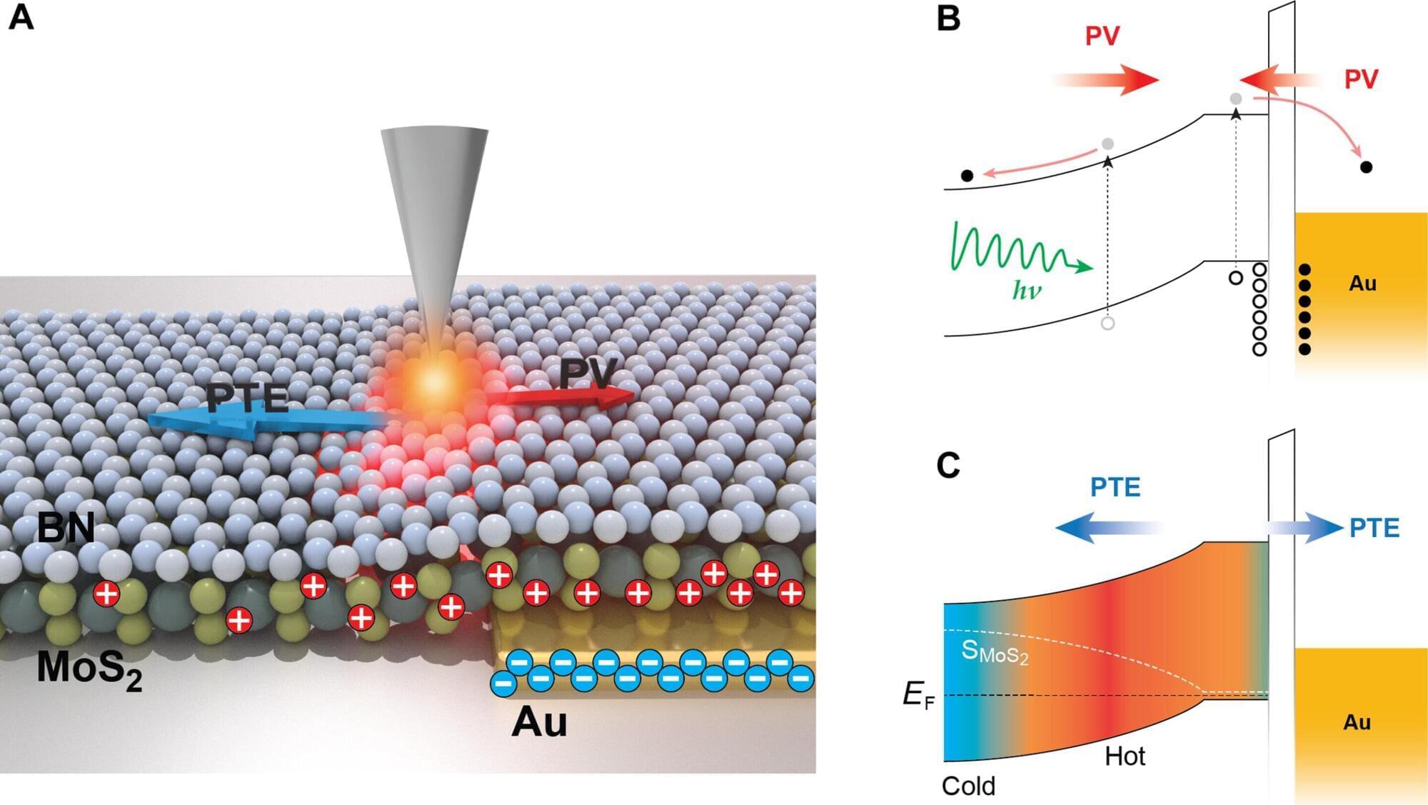
Engineers at EPFL have developed a device capable of transforming heat into electrical voltage efficiently at temperatures even colder than those found in outer space. This breakthrough could significantly advance quantum computing technologies by addressing a major obstacle.

To perform quantum computations, quantum bits (qubits) need to be cooled to temperatures in the millikelvin range (close to-273 degrees Celsius) to reduce atomic motion and minimize noise. However, the electronics used to control these quantum circuits generate heat, which is challenging to dissipate at such low temperatures. Consequently, most current technologies must separate the quantum circuits from their electronic components, resulting in noise and inefficiencies that impede the development of larger quantum systems beyond the laboratory.

Researchers in EPFL’s Laboratory of Nanoscale Electronics and Structures (LANES), led by Andras Kis, in the School of Engineering have now fabricated a device that not only operates at extremely low temperatures, but does so with efficiency comparable to current technologies at room temperature.

Purdue University material engineers have created a patent-pending process to develop ultrahigh-strength aluminum alloys that are suitable for additive manufacturing because of their plastic deformability.

Haiyan Wang and Xinghang Zhang lead a team that has introduced transition metals cobalt, iron, nickel and titanium into via nanoscale, laminated, deformable intermetallics. Wang is the Basil S. Turner Professor of Engineering and Zhang is a professor in Purdue’s School of Materials Engineering. Anyu Shang, a materials engineering graduate student, completes the team.

“Our work shows that the proper introduction of heterogenous microstructures and nanoscale medium-entropy intermetallics offers an alternative solution to design ultrastrong, deformable aluminum alloys via additive manufacturing,” Zhang said. “These alloys improve upon traditional ones that are either ultrastrong or highly deformable, but not both.”

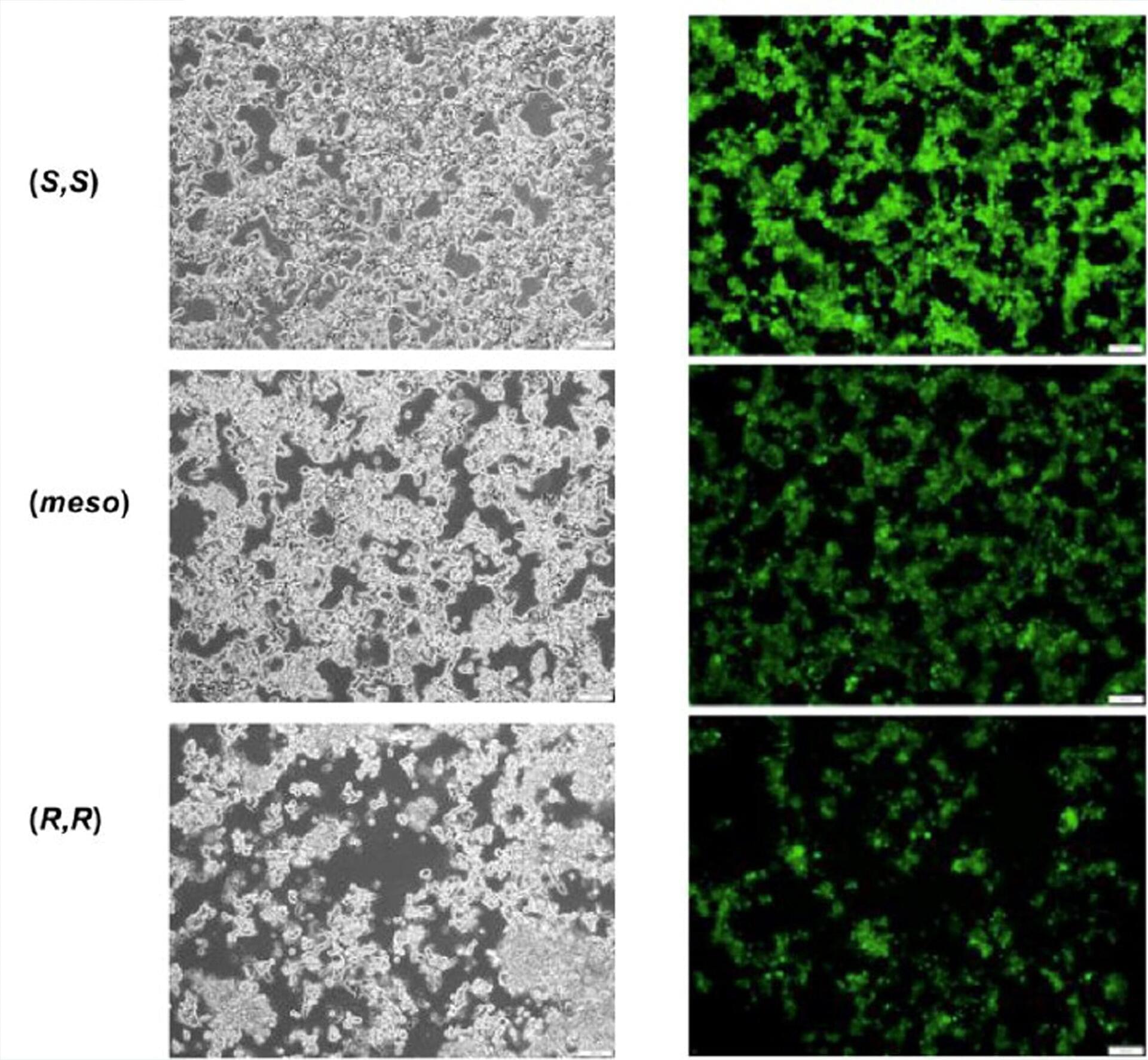
Up to 3% of people with diabetes have an allergic reaction to insulin. A team at Forschungszentrum Jülich has now studied a method that could be used to deliver the active substance into the body in a masked form—in the form of tiny nanoparticles.

The insulin is only released in the target organ when the pH value deviates from the slightly alkaline environment in the blood. The molecular transport system could also serve as a platform for releasing other drugs in the body precisely at the target site.

It’s an old dream in pharmacy: To deliver an active ingredient to the exact place in the body where it is most needed—a cancer drug, for example, directly to the tumor tissue. This minimizes its side effects on other organs and ensures that it has its maximum effect at its target.

Researchers at Finland’s Aalto University have found a way to use magnets to line up bacteria as they swim. The approach offers more than just a way to nudge bacteria into order – it also provides a useful tool for a wide range of research, such as work on complex materials, phase transitions and condensed matter physics.

The findings have been reported in Communications Physics (“Magnetically controlled bacterial turbulence”).

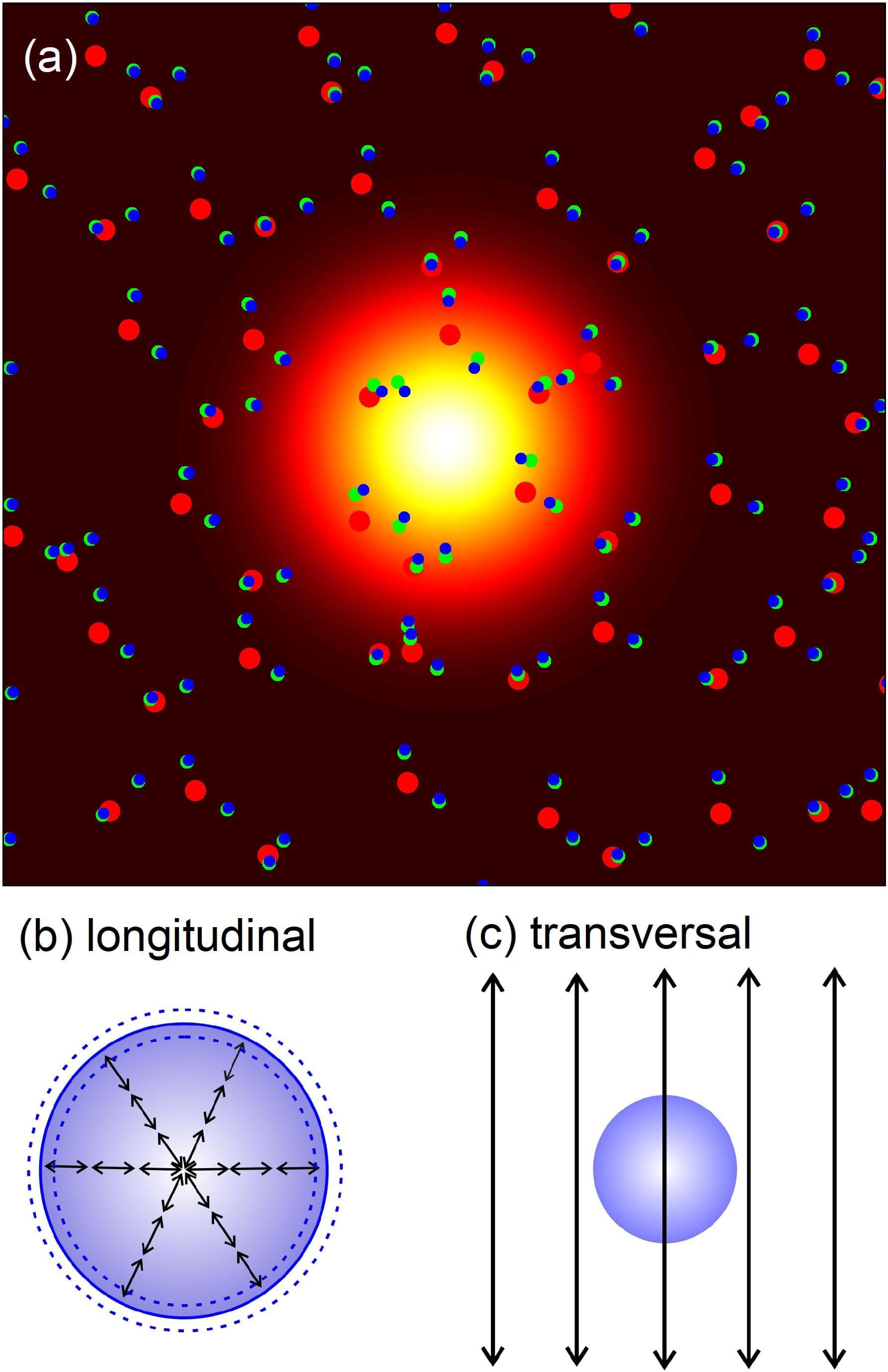
Bacterial cells generally aren’t magnetic, so the magnets don’t directly interact with the bacteria. Instead, the bacteria are mixed into a liquid with millions of magnetic nanoparticles. This means the rod-shaped bacteria are effectively non-magnetic voids inside the magnetic fluid. When the magnets are switched on, creating a magnetic field, the bacteria are nudged to line up with the magnetic field because any other arrangement takes more energy – it’s harder to keep the rod-shaped holes at an angle to the magnetic field.

Gallium nitride (GaN)-based light-emitting diodes (LEDs) have transformed the lighting industry by replacing conventional lighting technologies with superior energy efficiency, longer operating life and greater environmental sustainability.

In recent years, considerable attention has been paid to the trend toward miniaturization of LEDs, driven by display devices, augmented reality, virtual reality, and other emerging technologies. Due to the lack of cost-effective native substrates, the presence of high threading dislocation density in heteroepitaxial films grown on sapphire substrate is a major limiting factor for device performance.

In addition, Fresnel reflections at the interface between epitaxy and substrate caused by abrupt changes in the refractive indices of the material reduce the light energy utilization.

Researchers at Nano Life Science Institute (WPI-NanoLSI), Kanazawa University report the 3D imaging of a suspended nanostructure. The technique used is an extension of atomic force microscopy and is a promising approach for visualizing various 3D biological systems.

Atomic force microscopy (AFM) was originally invented for visualizing surfaces with nanoscale resolution. Its basic working principle is to move an ultrathin tip over a sample’s surface. During this xy-scanning motion, the tip’s position in the direction perpendicular to the xy-plane follows the sample’s height profile, resulting in a height map of the surface.

In recent years, ways to extend the method to 3D imaging have been explored, with researchers from Nano Life Science Institute (WPI-NanoLSI), Kanazawa University reporting pioneering experiments on living cells. However, for 3D-AFM to evolve into a widely applicable technique for visualizing flexible molecular structures, a thorough understanding of the imaging mechanisms at play is necessary.

Why it matters: Moore’s Law might not be dead after all. A new technique using nanomaterials can further miniaturize transistors, allowing fab plants to pack more of them on each chip. This research opens up new possibilities for creating advanced semiconductor devices with features smaller than current lithography techniques allow.

A South Korean research team led by Director Jo Moon-Ho of the Center for Van der Waals Quantum Solids within South Korea’s Institute for Basic Science has made a significant advancement in semiconductor and nanomaterial technology that could lead to the development of much smaller, more efficient, and more powerful electronic devices. The new technique can grow “one-dimentional” metallic nanaomaterials with widths as narrow as 0.4 nanometers for use as gate electrodes on 2D substrates. The technique promises to overcome the limitations of traditional lithography.

Integrated devices based on two-dimensional semiconductors exhibit excellent electrical properties even when thinned to atomic-scale thickness, making them promising candidates for creating ultra-thin, high-performance electronic devices. A separate study indicates that these 2D logic circuits are promising candidates for the post-Moore’s Law era.

Researchers have developed a genetic algorithm for designing phononic crystal nanostructures, significantly advancing quantum computing and communications.

The new method, validated through experiments, allows precise control of acoustic wave propagation, promising improvements in devices like smartphones and quantum computers.

Quantum Computing Revolution

PRESS RELEASE — To perform quantum computations, quantum bits (qubits) must be cooled down to temperatures in the millikelvin range (close to-273 Celsius), to slow down atomic motion and minimize noise. However, the electronics used to manage these quantum circuits generate heat, which is difficult to remove at such low temperatures. Most current technologies must therefore separate quantum circuits from their electronic components, causing noise and inefficiencies that hinder the realization of larger quantum systems beyond the lab.

Researchers in EPFL’s Laboratory of Nanoscale Electronics and Structures (LANES), led by Andras Kis, in the School of Engineering have now fabricated a device that not only operates at extremely low temperatures, but does so with efficiency comparable to current technologies at room temperature.