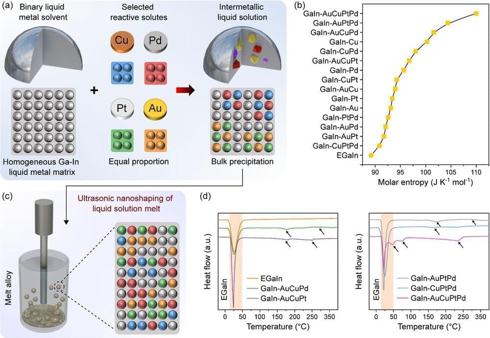
Researchers synthesize high-entropy liquid metal alloys at nanoscale, achieving atomic dispersion of noble metals and demonstrating enhanced catalytic activity for hydrogen evolution.
Category: nanotechnology – Page 46
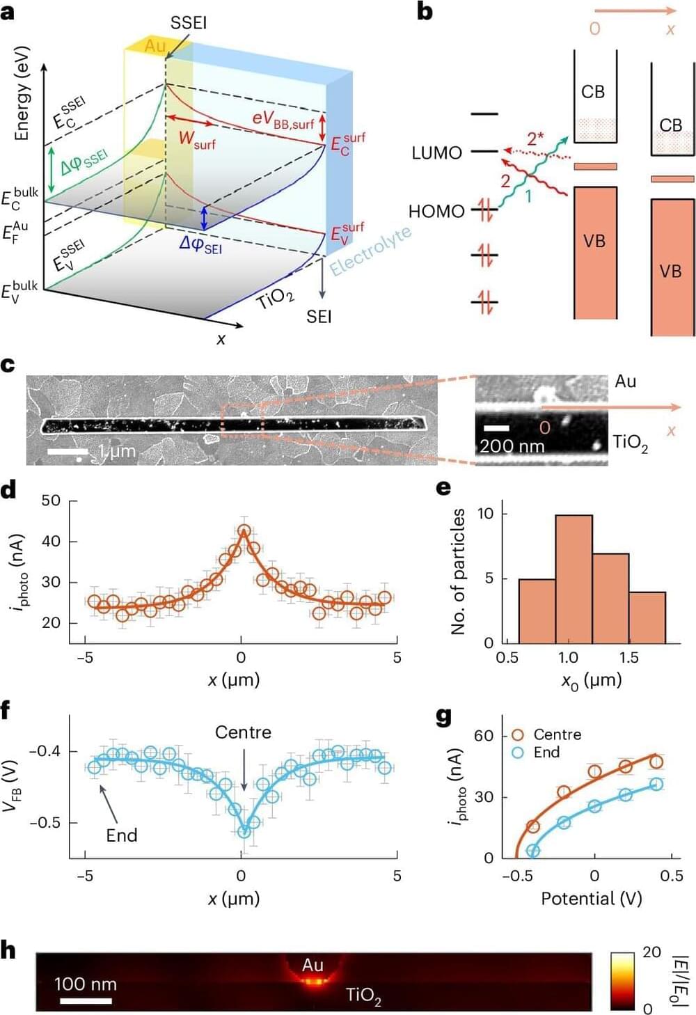
To remove micropollutants such as pesticides and trace chemicals from the environment, you need something equally small and cunning. One potential method is photocatalysis, which uses semiconducting nanomaterials powered by sunlight to adsorb toxic chemicals on the materials’ surface and degrade them.
Successfully innovating optoelectronic semiconductor devices depends a lot on moving charges and excitons—electron-hole pairs—in specified directions for the purpose of creating fuels or electricity.
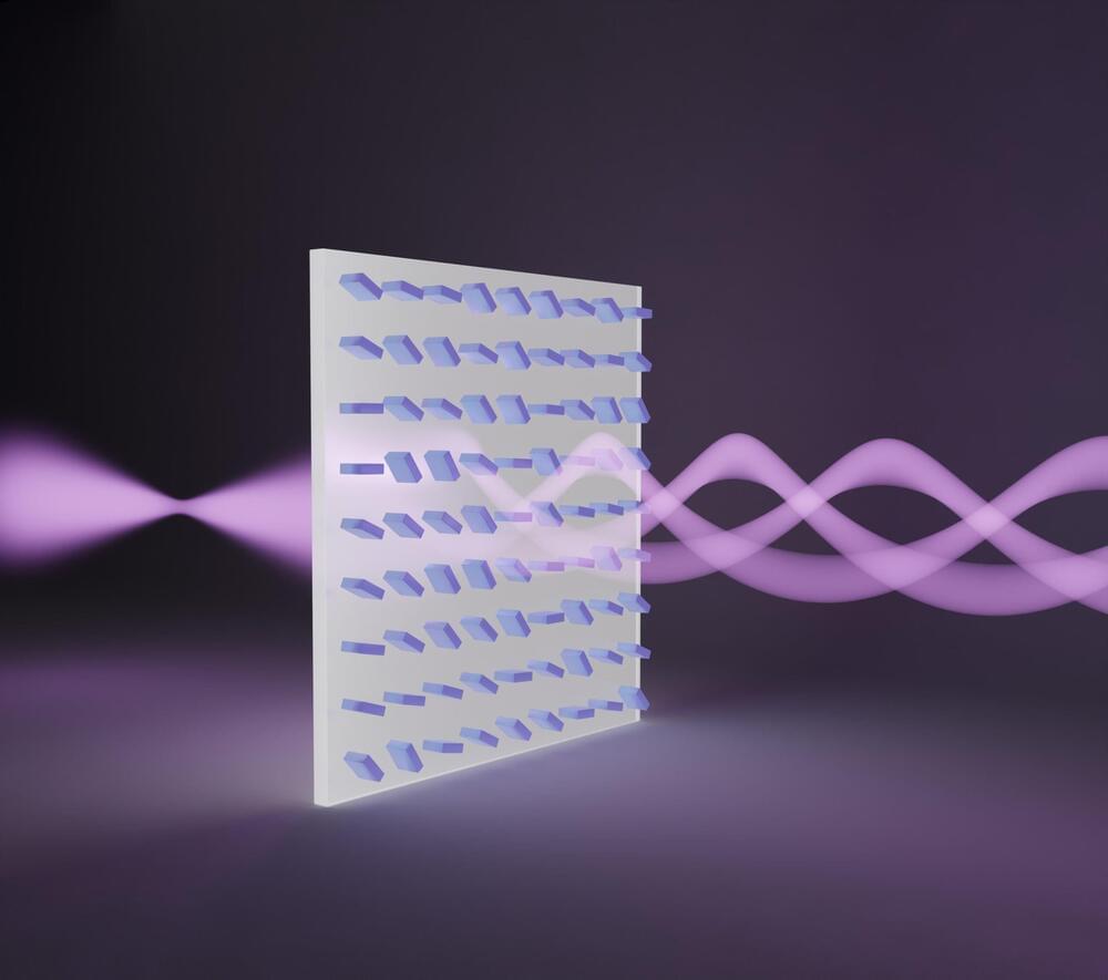
Researchers at TMOS have developed a metasurface-enabled solenoid beam that can pull particles towards it, potentially revolutionizing non-invasive medical procedures like biopsies. This technology, which uses a thin layer of nanopatterned silicon, offers a lightweight, portable alternative to the bulky equipment previously required for such beams. Credit: University of Melbourne.
Researchers at TMOS, the ARC Centre of Excellence for Transformative Meta-Optical Systems, have made a significant initial advancement in creating tractor beams enabled by metasurfaces. These beams of light, capable of drawing particles towards them, are inspired by the fictional tractor beams seen in science fiction.
In research published in ACS Photonics, the University of Melbourne team describes their solenoid beam that is generated using a silicon metasurface. Previous solenoid beams have been created by bulky special light modulators (SLMs), however, the size and weight of these systems prevent the beams from being used in handheld devices. The metasurface is a layer of nanopatterned silicon only about 1/2000 of a millimeter thick. The team hopes that one day it could be used to take biopsies in a non-invasive manner, unlike current methods such as forceps that cause trauma to the surrounding tissues.
Unlocking the brain: how magnetic nanomaterials could transform neuroscience.
Mind-control magnet tech to regulate behavior, emotions, hunger.
Understanding the brain’s intricate networks and functions is a complex challenge.
Using magnetic fields and nanoparticles, researchers were able to increase and decrease feeding behavior and appetite in mice models.
A new method enables precise nanofabrication inside silicon using spatial light modulation and laser pulses, creating advanced nanostructures for potential use in electronics and photonics.
Silicon, the cornerstone of modern electronics, photovoltaics, and photonics, has traditionally been limited to surface-level nanofabrication due to the challenges posed by existing lithographic techniques. Available methods either fail to penetrate the wafer surface without causing alterations or are limited by the micron-scale resolution of laser lithography within Si.
In the spirit of Richard Feynman’s famous dictum, ‘There’s plenty of room at the bottom’, this breakthrough aligns with the vision of exploring and manipulating matter at the nanoscale. The innovative technique developed by the Bilkent team surpasses current limitations, enabling controlled fabrication of nanostructures buried deep inside silicon wafers with unprecedented control.
Nanotechnology is an exciting new area in science, with many possible applications in medicine. This article seeks to outline the role of different areas such as diagnosis of diseases, drug delivery, imaging, and so on.
Researchers develop methods to dramatically increase light emission from nitrogen-vacancy centers in nanodiamonds, advancing quantum sensing and bioimaging applications.
Small-angle scattering (SAS) is a powerful technique for studying nanoscale samples. So far, however, its use in research has been held back by its inability to operate without some prior knowledge of a sample’s chemical composition. Through new research published in The European Physical Journal E, Eugen Anitas at the Bogoliubov Laboratory of Theoretical Physics in Dubna, Russia, presents a more advanced approach, which integrates SAS with machine learning algorithms.
face_with_colon_three year 2023.
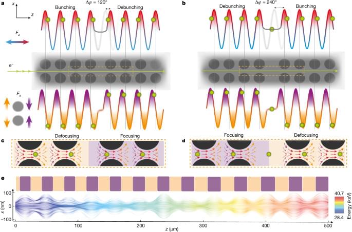
A scalable nanophotonic electron accelerator with a high particle acceleration gradient and good beam confinement achieves an energy gain of 43%.
