A new “drug” uses magnetically-driven nanoparticles to both stop bleeding and reduce blood loss from internal bleeding, which is often fatal.

A research team composed of scientists from the Institute of Bioengineering and Nanotechnology (IBN) of the Agency for Science, Technology and Research (A*STAR) and IBM Research has produced a new synthetic molecule that can target and kill five multidrug-resistant bacteria. This synthetic polymer was found to be non-toxic and could enable entirely new classes of therapeutics to address the growing problem of antibiotic-resistant superbugs.
The synthetic molecules are called guanidinium-functionalized polycarbonates and were found to be both biodegradable and non-toxic to human cells. Essentially, the positively-charged synthetic polymer enters a living body and binds specifically to certain bacteria cells by homing in on a microbial membrane’s related negative charge. Once attached to the bacteria, the polymer crosses the cell membrane and triggers the solidification of proteins and DNA in the cell, killing the bacteria.

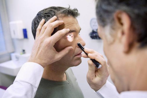
Eye-drops that can repair the corneas and can improve the short and long sightedness have been developed by a team of Ophthalmologists at Shaare Zedek Medical Center and Bar-Ilan University’s Institute of Nanotechnology and Advanced Materials. The solution of nanoparticles called the ‘nanodrops’ was successfully tested on a pig’s cornea. Clinical trials are expected to be carried out later this year. If the clinical trials on humans are successful, it is expected that the need of eyeglasses will be eliminated.
The leader of the research team, Dr. David Smadja, said that the eye-drops can bring a revolution in ophthalmological and optometry treatment of patients who are suffering from myopia, hyperopia and other refractory conditions. The revolutionary breakthrough in the field was revealed by Dr. Smadja at Shaare Zedek’s second biennial research day, which was held at Steinberg Auditorium in Jerusalem. He said that the nano drops can also be used to replace multifocal lenses and allow people to see objects from different distances. Smadja said, “This is a new concept for correcting refractory problems.” However, he didn’t mention the times of applications which will replace the need for the glasses completely.
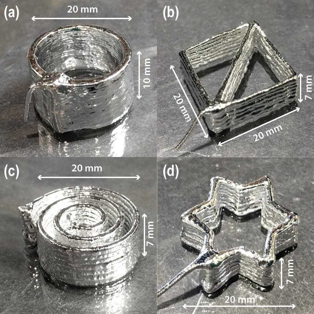
Researchers in Oregon State University’s College of Engineering have taken a key step toward the rapid manufacture of flexible computer screens and other stretchable electronic devices, including soft robots.
The advance by a team within the college’s Collaborative Robotics and Intelligent Systems Institute paves the way toward the 3D printing of tall, complicated structures with a highly conductive gallium alloy.
Researchers put nickel nanoparticles into the liquid metal, galinstan, to thicken it into a paste with a consistency suitable for additive manufacturing.

The researchers also suggested that aliens could “gift” us with an artificial intelligence (AI) system that may trick humans into developing self-replicating nanobots and eventually deploy them to wreak havoc on our planet. The researchers argue that it would be cheaper for aliens to “send a malicious message to eradicate humans compared to sending battleships”.
In one scenario, the researchers argued that a message from aliens could be a panic-inducing statement like “We will make your sun go supernova tomorrow”. According to the researchers, if such a threatening message is received in just one location, it may be possible to contain and even destroy it. “If it is received repeatedly, perhaps even by amateurs, containment is impossible,” the researchers wrote in a paper available online on arXiv.
In another scenario, the scientists argue that humans could be tricked into begetting their own demise by aliens offering the “gift” of knowledge. For instance, aliens could transmit a message that reads: “We are friends. The galactic library is attached. It is in the form of an artificial intelligence (AI) which quickly learns your language and will answer your questions. You may execute the code following these instructions…”
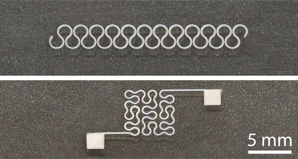
Researchers at North Carolina State University have developed a new technique that allows them to print circuits on flexible, stretchable substrates using silver nanowires. The advance makes it possible to integrate the material into a wide array of electronic devices.
Silver nanowires have drawn significant interest in recent years for use in many applications, ranging from prosthetic devices to wearable health sensors, due to their flexibility, stretchability and conductive properties. While proof-of-concept experiments have been promising, there have been significant challenges to printing highly integrated circuits using silver nanowires.
Silver nanoparticles can be used to print circuits, but the nanoparticles produce circuits that are more brittle and less conductive than silver nanowires. But conventional techniques for printing circuits don’t work well with silver nanowires; the nanowires often clog the printing nozzles.
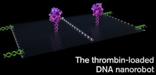
In a major advancement in nanomedicine, Arizona State University (ASU) scientists, in collaboration with researchers from the National Center for Nanoscience and Technology (NCNST), of the Chinese Academy of Sciences, have successfully programmed nanorobots to shrink tumors by cutting off their blood supply.

Researchers at the University of Chicago have developed light-activated nanowires that can stimulate neurons to fire when they are exposed to light. The researchers hope that the nanowires could help in understanding complex brain circuitry, and they may also be useful in treating brain disorders.
Optogenetics, which involves genetically modifying neurons so that they are sensitive to a light stimulus, has attracted a lot of attention as a research tool and potential therapeutic approach. However, some researchers have misgivings about optogenetics, as it involves inserting a gene into cells, potentially opening the door to unforeseen effects and possibly permanently altering treated cells.
In an effort to develop an alternative, a research team at the University of Chicago has devised a new modality that can enable light activation of neurons without the need for genetic modification. Their technique involves nanowires that are so small that if they were laid side-by-side, hundreds of them would fit on the edge of a sheet of paper. Although initially designed for use in solar cells, their small size also makes them well suited to interacting with cells.
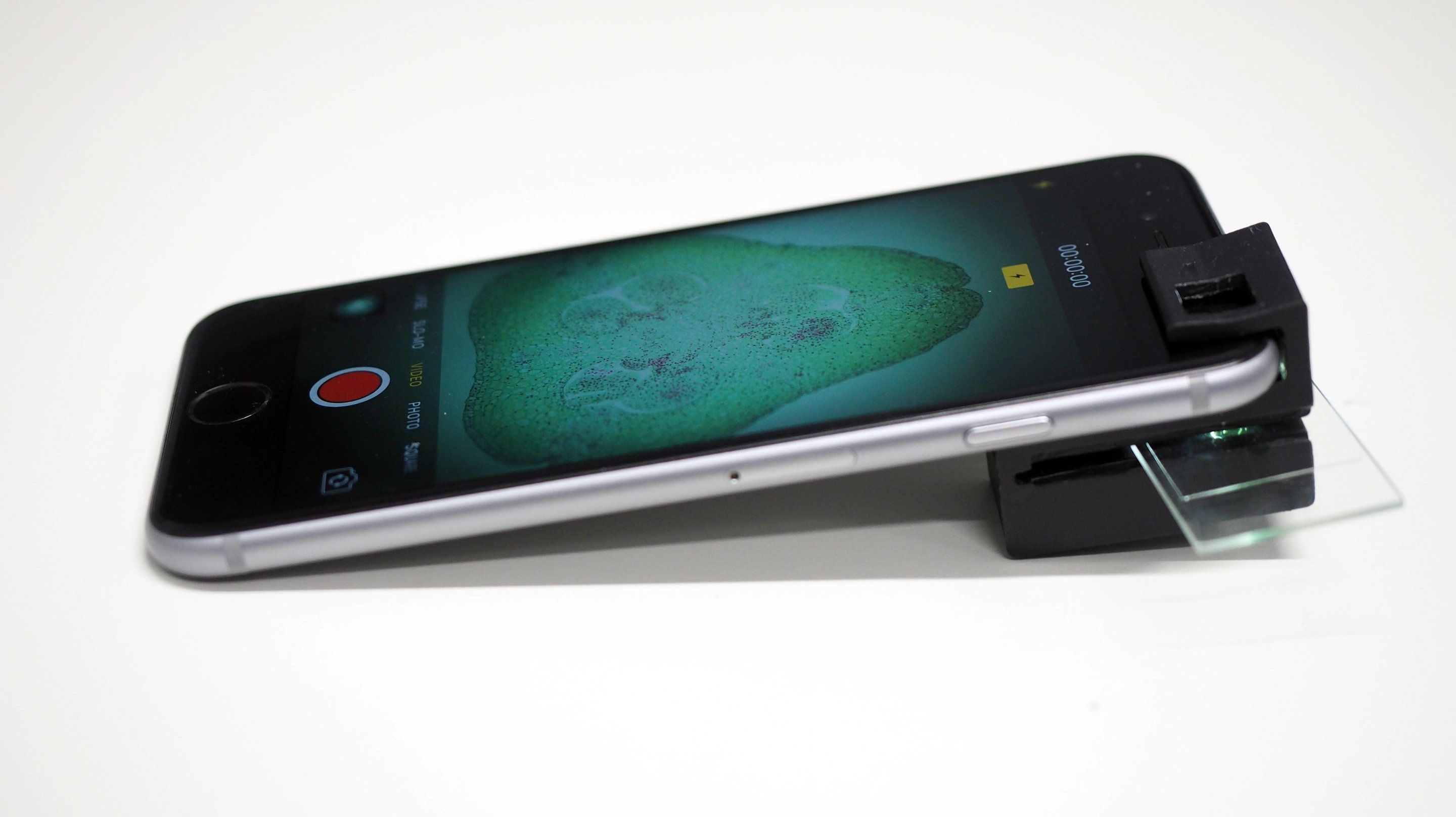
Australian researchers from the ARC Centre of Excellence for Nanoscale BioPhotonics (CNBP) have developed a 3D printable ‘clip-on’ that can turn any smartphone into a fully functional microscope.
Reported in the research journal Scientific Reports, the smartphone microscope is powerful enough to visualise specimens as small as 1/200th of a millimetre, including microscopic organisms, animal and plant cells, blood cells, cell nuclei and more.
The clip-on technology is unique in that it requires no external power or light source to work yet offers high-powered microscopic performance in a robust and mobile handheld package.