Nanoscience is now redefining how light can be controlled and processed on chip.

In a multi-institutional study published today in Nature Nanotechnology, researchers from The University of Texas MD Anderson Cancer Center reported that engineered bispecific nanobodies successfully strengthened mucosal defenses in the respiratory tract, improving protection against influenza infection and reducing SARS-CoV-2 transmission in vivo.
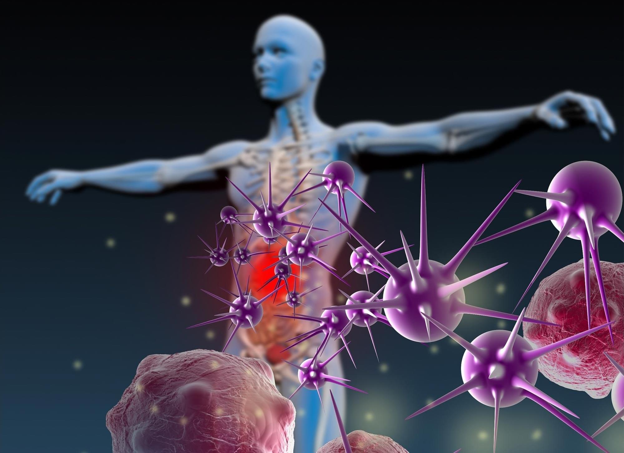
Wen Jiang, M.D., Ph.D., associate professor of Radiation Oncology, has been researching different nanotechnologies for their potential use in delivering cancer therapies. That research has led to work with Liming Zhou, M.D., a postdoctoral student, and the late Charles Chan, Ph.D., assistant professor of surgery at Stanford Medicine.
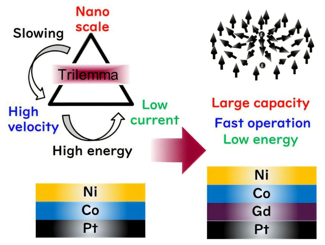
Researchers at Kyushu University have shown that careful engineering of materials interfaces can unlock new applications for nanoscale magnetic spins, overcoming the limits of conventional electronics. Their findings, published in APL Materials, open up a promising path for tackling a key challenge in the field and ushering in a new era of next-generation information devices.
The study centers around magnetic skyrmions—swirling, nanoscale magnetic structures that behave like particles. Skyrmions possess three key features that make them useful as data carriers in information devices: nanoscale size for high capacity, compatibility with high-speed operations in the GHz range, and the ability to be moved around with very low electrical currents.
A skyrmion-based device could, in theory, surpass modern electronics in applications such as large-scale AI computing, Internet of Things (IoT), and other big data applications.
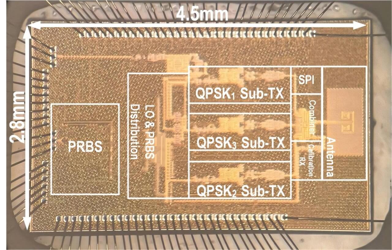
A new transceiver invented by electrical engineers at the University of California, Irvine boosts radio frequencies into 140-gigahertz territory, unlocking data speeds that rival those of physical fiber-optic cables and laying the groundwork for a transition to 6G and FutureG data transmission protocols.
To create the transceiver, researchers in UC Irvine’s Samueli School of Engineering devised a unique architecture that blends digital and analog processing. The result is a silicon chip system, comprising both a transmitter and a receiver, that’s capable of processing digital signals significantly faster and with much greater energy efficiency than previously available technologies.
The team from UC Irvine’s Nanoscale Communication Integrated Circuits Labs outline its work in two papers published this month in the IEEE Journal of Solid-State Circuits. In one, the engineers discuss the technology they call a “bits-to-antenna” transmitter, and in the second, they cover their “antenna-to-bits” receiver.
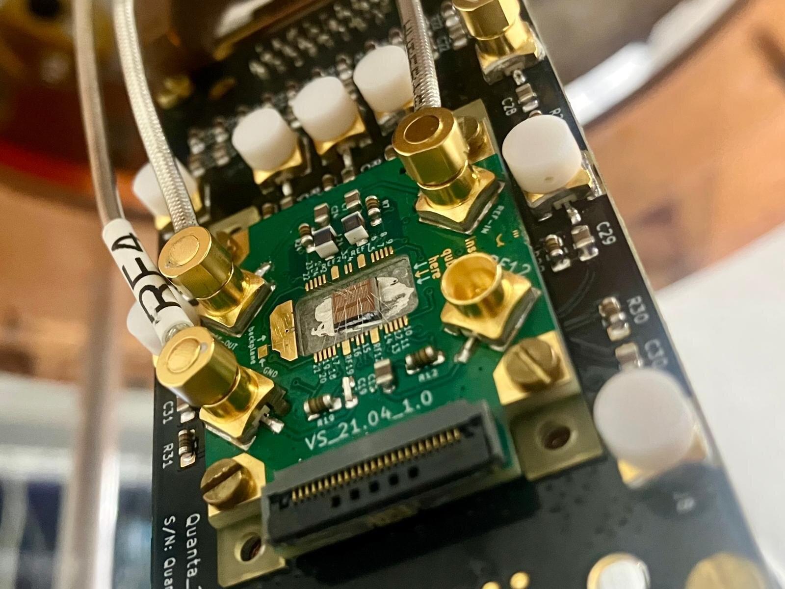
Quantum computers, systems that process information leveraging quantum mechanical effects, could reliably tackle various computational problems that cannot be solved by classical computers. These systems process information in the form of qubits, units of information that can exist in two states at once (0 and 1).
Hole spins, the intrinsic angular momentum of holes (i.e., missing electrons in semiconductors that can be trapped in nanoscale regions called quantum dots), have been widely used as qubits. These spins can be controlled using electric fields, as they are strongly influenced by a quantum effect known as spin-orbit coupling, which links the motion of particles to their magnetism.
Unfortunately, due to this spin-orbit coupling, hole spin qubits are also known to be highly vulnerable to noise, including random electrical disturbances that can prompt decoherence. This in turn can result in the loss of valuable quantum information.
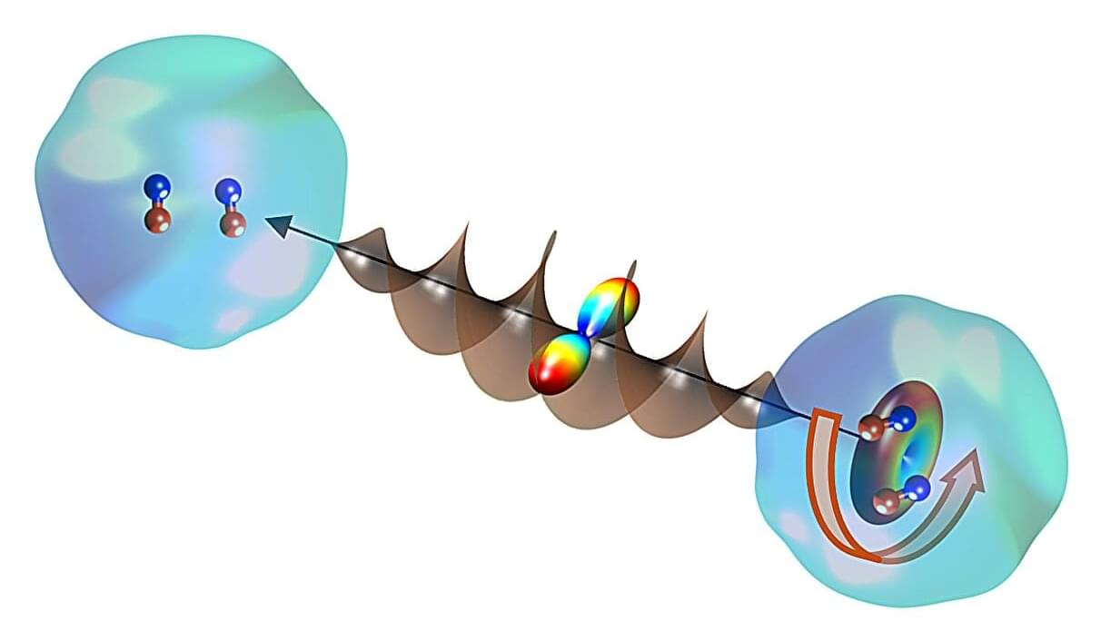
Physicists have used a new optical centrifuge to control the rotation of molecules suspended in liquid helium nano-droplets, bringing them a step closer to demystifying the behavior of exotic, frictionless superfluids.
It’s the first demonstration of controlled spinning inside a superfluid—researchers can now directly set the direction and frequency of the molecule’s rotation, which is vital in studying how molecules interact with the quantum environment at various rotational frequencies. The method was outlined this week by researchers at the University of British Columbia (UBC) and colleagues at the University of Freiburg in the journal Physical Review Letters.
“Controlling the rotation of a molecule dissolved in any fluid is a challenge,” said Dr. Valery Milner, associate professor with UBC Physics and Astronomy and lead author on the paper.
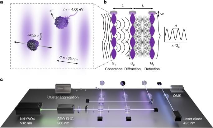
Can a small lump of metal be in a quantum state that extends over distant locations? A research team at the University of Vienna answers this question with a resounding yes. In the journal Nature, physicists from the University of Vienna and the University of Duisburg-Essen show that even massive nanoparticles consisting of thousands of sodium atoms follow the rules of quantum mechanics. The experiment is currently one of the best tests of quantum mechanics on a macroscopic scale.
In quantum mechanics, not only light but also matter can behave both as a particle and as a wave. This has been proven many times for electrons, atoms, and small molecules through double-slit diffraction or interference experiments. However, we do not see this in everyday life: marbles, stones, and dust particles have a well-defined location and a predictable trajectory; they follow the rules of classical physics.
At the University of Vienna, the team led by Markus Arndt and Stefan Gerlich has now demonstrated for the first time that the wave nature of matter is also preserved in massive metallic nanoparticles. The scale of the particles is impressive: the clusters have a diameter of around 8 nanometers, which is comparable to the size of modern transistor structures.