As someone with a passionate interest in longevity, transhumanism and biological immortality — I am naturally both excited and optimistic that medical technology will continue to advance in my lifetime — hopefully to the point where humanity has cured or at least greatly mitigated the signs & symptoms of most diseases as well as disabilities, radically expanded human biological lifespan regardless of age, and created a more dignified existence for all as a result of rapid breakthroughs in robotics, AI, automation, nanotechnology, 3D printing and biotechnology — which I hope in turn will largely eradicate poverty, disease, food & shelter insecurity, natural resource scarcity, environmental degradation and income inequality. I know that some of my likeminded friends are far more skeptical that we will ever see outright cures or significant mitigations for major diseases and disabilities — much less radical life extension or perhaps biological immortality in human beings — which are widely available on a commercial basis. They cite their belief that pharmaceutical giants, a plethora of not for profit organizations (i.e., American Cancer Society), and many other allegedly “self-interested parties” supposedly allied with government regulatory bodies — apparently do not want to see diseases or disabilities cured or lifespan significantly extended — EVER — as this would prevent them from earning untold sums selling treatments and supports for such things on a regular ongoing basis (i.e., chemo drugs for cancer, statins for cardiovascular disease, inhaled/oral steroids for lung disease, renal replacement therapy for kidney disease, mobile supports for spinal cord injuries, ect.) They believe that too much money would be at stake, too many jobs on the line and the entire “pharma-medical-academic industrial complex” supposedly at great risk, if actual cures or significant mitigations ever saw the light of day. Some of these friends even cite their belief that fully autonomous, accident proof, self-driving cars will most likely never occur — as it would supposed put the entire auto insurance industry at existential risk as well as deprive law enforcement agencies of a key source of reliable revenue (issuing speeding tickets) This one makes me giggle! 🤭 My friends also believe that radical life extension in human beings — much less biological immortality — would apparently upset the proverbial apple cart — where the “powers that be” are concerned — in terms of everything from the highly lucrative profits which are derived from pharmaceutical sales, old age homes, life and health insurance plans, personal financial services and all of the sales of key products and services associated with the aging process — to macroeconomic considerations such as the long term viability of government entitlement programmes. They believe that government regulatory authorities allegedly working at the behest of the aforementioned self-interested parties will always seek to delay, disrupt or even derail ANY and ALL significant progress into cures/mitigations for disease/disabilities, radical human life extension and/or human biological immortality. Apparently, new biotech start ups which do advance the aforementioned things are allegedly “always aggressively bought out by monopoly capital — with their cures and advances indefinitely suppressed” I personally tend to be more on the positive and optimistic side where these things are concerned — but perhaps these rather pessimistic arguments do have some validity — minus the implied conspiracy theory aspect. Do you think human beings will ever be “allowed” to truly be free from illnesses and disabilities? Will we ever be “permitted” to radically expand our lifespans or even become biologically immortal at some point? Please discuss.
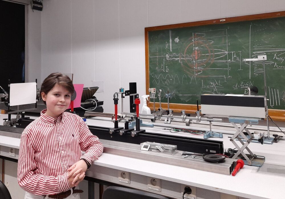
I have already taken a few courses for a master’s in physics at the University of Antwerp and I want to complete it there. In a bachelor’s degree you get a basis of knowledge in physics and quantum physics, but it gets more detailed in a master’s.
The main reason I chose to study physics is because my end goal is to achieve immortality. One of the areas that is important in the study of immortality is physics, but as of yet, there is no mapped out path to achieve it.
I am interested in immortality because my grandparents suffer from heart disease. I want to help them and I want to help other kids so they don’t have to lose their grandparents. You could look at immortality as a very big puzzle. We have a lot of pieces of the puzzle, which are different studies and research, and it’s possible that combining the knowledge from those studies will develop new insights and ideas. Something I am interested in is artificial organs; I would like to be able to replace as many parts of the body as possible with artificial organs. I plan to do a lot of studying, gather a lot of knowledge and then all the pieces will hopefully fit in together and the puzzle of immortality may be solved.

