Alloys that can return to their original structure after being deformed have a so-called shape memory. This phenomenon and the resulting forces are used in many mechanical actuating systems, for example in generators or hydraulic pumps. However, it has not been possible to use this shape-memory effect at a small nanoscale. Objects made of shape-memory alloy can only change back to their original shape if they are larger than around 50 nanometers.
Researchers led by Salvador Pané, Professor of Materials of Robotics at ETH Zurich, and Xiang-Zhong Chen, a senior scientist in his group, were able to circumvent this limitation using ceramic materials. In a study published in the journal Nature Communications, they demonstrate the shape-memory effect on a layer that is about twenty nanometers thick and made of materials called ferroic oxides. This achievement now makes it possible to apply the shape-memory effect to tiny nanoscale machines.
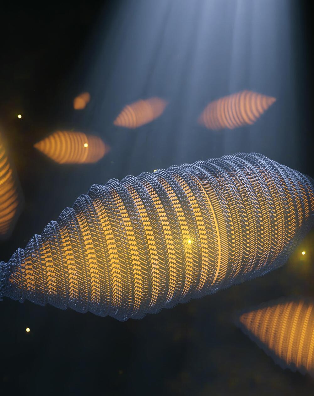
At first glance, ferroic oxides do not appear to be very suitable for the shape-memory effect: They are brittle in bulk scale, and in order to produce very thin layers of them, they usually have to be fixed onto a substrate, which makes them inflexible. In order to still be able to induce the shape-memory effect, the researchers used two different oxides, barium titanate and cobalt ferrite, of which they temporarily applied thin layers onto a magnesium oxide substrate. The lattice parameters of the two oxides differ significantly from each other. After the researchers had detached the two-layered strip from the supporting substrate, the tension between the two oxides generated a spiral-shaped twisted structure.