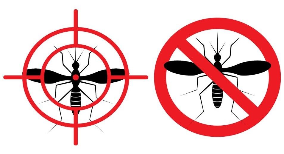
Toggle light / dark theme

Change is coming; will you be ready?
I remember many decades ago when folks were trying to learn a new OS that changed businesses, governments/ educational institutions, and households around the world. That OS was called Windows; and hearing the stories as well as watching people try to use a PC and a mouse was interesting then.

Now, the world will again go through a large scale metamorphosis again when more and more QC is evolved and made available over the next 5 to 7 years in the technology mainstream. Change is often necessary and often can be good as well.


You might ask yourself, “What is quantum computing, and how do I get involved?”

Before we begin to explain quantum computing, a brief glimpse of the past is essential to understand how quantum computing came to be.

New Russian technologies, including phonecall interception and a facial recognition app, have stirred a fierce debate about privacy and data monitoring.

Infowatch, a Moscow-based IT security company managed by businesswoman Natalya Kasperskaya, found itself in hot water last month after it revealed it had invented a system that companies can use to intercept employees’ mobile phone conversations.

Companies outside Russia have also devised call interception software, and Infowatch already markets products that monitor employees’ e-mails, USB keys and printers.

Read more

If you’ve ever held a high-quality camera lens, the first thing you notice is the weight. Thanks to layers and layers of thick glass hunks inside, they end up being very heavy. However, thanks to research being done at Harvard on something called metalenses, one day those mgiant glass-filled lenses might be obsolete.

The curved surfaces on a glass lens focus incoming light onto a camera’s digital sensor. The more precise (and expensive) the lens is, the better the image it will produce.

Metalenses work in a similar way, but they’re not made of precision-ground glass. Instead, a layer of transparent quartz is completely covered in a layer of tiny towers made from titanium dioxide. When arranged in specific patterns, those complex tower arrays can focus light exactly like a glass lens does. Except that these tiny metalenses end up being thinner than a human hair, and weigh almost nothing.

Read more

Nice!


Metal organic vapor phase deposition on etched 4-inch-diameter sapphire wafers is used to create low-defect-density gallium nitride templates.

Visible emitting LEDs based on gallium nitride (GaN) materials have made tremendous progress since their initial development in the early 1990s. Indeed, these LEDs are now in everyday use in many applications, e.g., for solid state lighting, and for backlighting in televisions and smartphones. LED technology, however, also has several inherent problems. These include decreasing efficiency under high injection current (droop), color change with increasing current, and poor efficiency in the green and yellow parts of the spectrum. These problems are associated with the natural polar (0001) crystal plane of wurtzite GaN, on which commercial LEDs are based, with the use of ‘c-plane’ sapphire substrates.

Read more

Intel is in the midst of its biggest business transition ever. Just a few months ago, the chip giant announced that it would be laying off 11,000 workers and taking a step away from the PC market. Instead, it’ll be focusing on wearables and IoT devices. Coinciding with those announcements was an executive shuffle that put Navin Shenoy, its Mobile Client VP, in charge of its wider Client Computing Group (which covers all consumer devices). At Computex this week, we had a chance to pick Shenoy’s brain about Intel’s path forward.

Taiwan Computex

What do you envision being the next major breakthrough for PC form factor?

We’re working on lots of things that are mind-blowing. To me, we have to figure out how to get to J.A.R.V.I.S. [Iron Man’s trusty AI, not Intel’s vaporware earpiece]. The ability to manipulate things wherever you are, look at things wherever you are, talk to things in a more natural way. That’s the next big breakthrough in computing. And it will be in so many domains, it won’t just be PCs. It’ll be phones, tablets and also new types of things we haven’t conceived of yet.

Read more

Scientists at Ludwig-Maximilians-Universitaet (LMU) in Munich and the Max Planck Institute for Quantum Optics (MPQ) have devised a new interferometer to probe the geometry of band structures.

The geometry and topology of electronic states in solids play a central role in a wide range of modern condensed-matter systems, including graphene and topological insulators. However, experimentally accessing this information has proven to be challenging, especially when the bands are not well isolated from one another. As reported by Tracy Li et al. in last week’s issue of Science (Science, May 27, 2016, DOI: 10.1126/science.aad5812), an international team of researchers led by Professor Immanuel Bloch and Dr. Ulrich Schneider at LMU Munich and the Max Planck Institute of Quantum Optics has devised a straightforward method with which to probe band geometry using ultracold atoms in an optical lattice. Their method, which combines the controlled transport of atoms through the energy bands with atom interferometry, is an important step in the endeavor to investigate geometric and topological phenomena in synthetic band structures.

A wide array of fundamental issues in condensed-matter physics, such as why some materials are insulators while others are metals, can be understood simply by examining the energies of the material’s constituent electrons. Indeed, band theory, which describes these electron energies, was one of the earliest triumphs of quantum mechanics, and has driven many of the technological advances of our time, from the computer chips in our laptops to the liquid-crystal displays on our smartphones. We now know, however, that traditional band theory is incomplete.

Read more

Storage in your laptop or smartphone is a compromise between volume, access speed and physical size. But, the industry’s competition to shrink them while boosting their specifications is fierce. A few months after shipping a 16TB solid-state drive, Samsung has announced a fast, efficient 512GB SSD that’s half the size of a postage stamp.

Samsung’s press release claims that the drive is the first mass-produced 512GB SSD with non-volatile memory express (NVMe), a host-controller interface with a streamlined register for speed, in a single package. Unlike other hard drives in multi-chip packages (MCP), Samsung’s new drive is organized in a ball grid array into a collected unit, making it simpler to fit in and connect to other parts in the device. This makes the drive ideal for the ultra-slim notebook PC market, where space and weight are at a premium.

A senior Samsung VP said in a press release that the tiny drive triples the performance of a typical SATA SSD. Its read/write speeds of up to 1,500MB/s and 900MB/s, respectively, mean you could transfer a 5GB HD video in 3 seconds. Samsung will start selling the drive in June in 512GB, 256GB and 128GB models.

Read more

Make no mistake, today’s wearables are clever pieces of kit. But they can be bulky and restricted by the devices they must be tethered to. This has led engineers to create thinner and more powerful pieces of wearable technology that can be applied directly to the skin. Now, researchers at the University of Wisconsin-Madison, led by Zhenqiang “Jack” Ma, have developed “the world’s fastest stretchable, wearable integrated circuits,” that could let hospitals apply a temporary tattoo and remove the need for wires and clips.

With its snake-like shape, the new platform supports frequencies in the .3 gigahertz to 300 gigahertz range. This falls in what is set to become the 5G standard. For a mobile phone, 5G enables faster speeds and greater coverage, but with epidermal electronics, engineers have discussed the possibility that wearers could transmit their vitals to a doctor without having to leave their home.

While the idea isn’t unique, the integrated circuits created by Ma and his team have a much smaller footprint than those developed by other researchers. Earlier transmission lines can measure up to 640 micrometers (or .64 millimeters), but UW–Madison’s solution is just 25 micrometers (or .025 millimeters) thick. The Air Force Office of Scientific Research also supports Ma’s research, suggesting that his wearable breakthroughs may help pilots of the future.

Read more