A particle called Pines’s demon has been seen inside a superconductor, decades after it was first predicted.
By Alex Wilkins
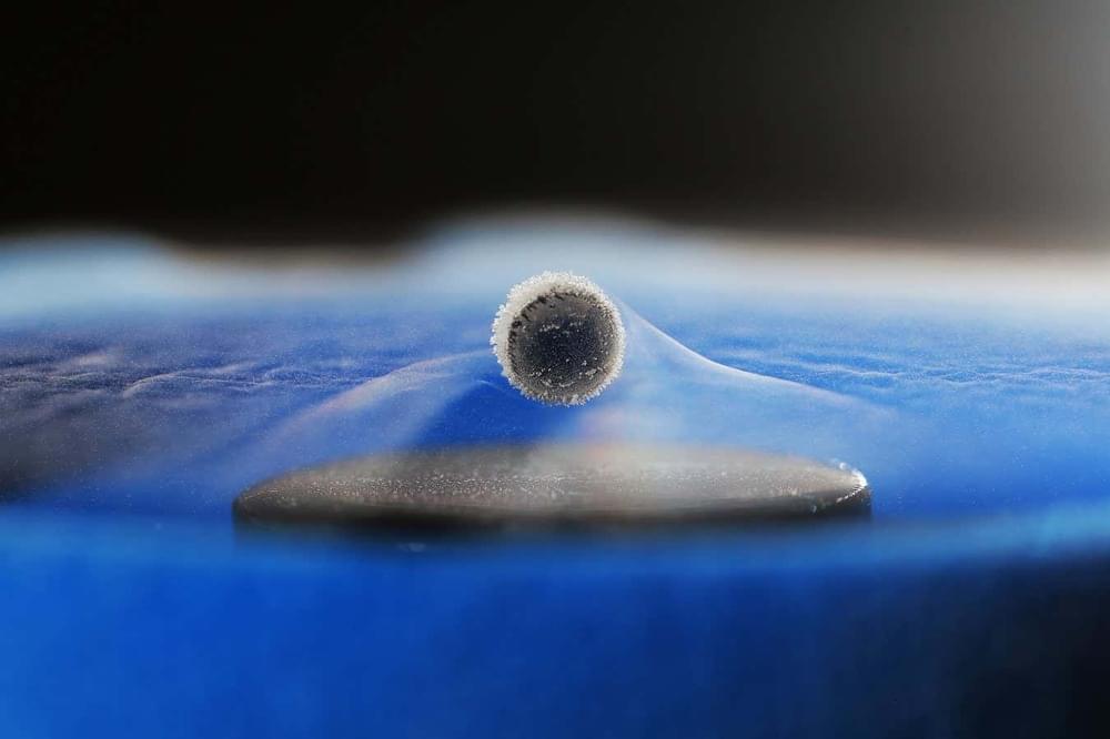
A particle called Pines’s demon has been seen inside a superconductor, decades after it was first predicted.
By Alex Wilkins
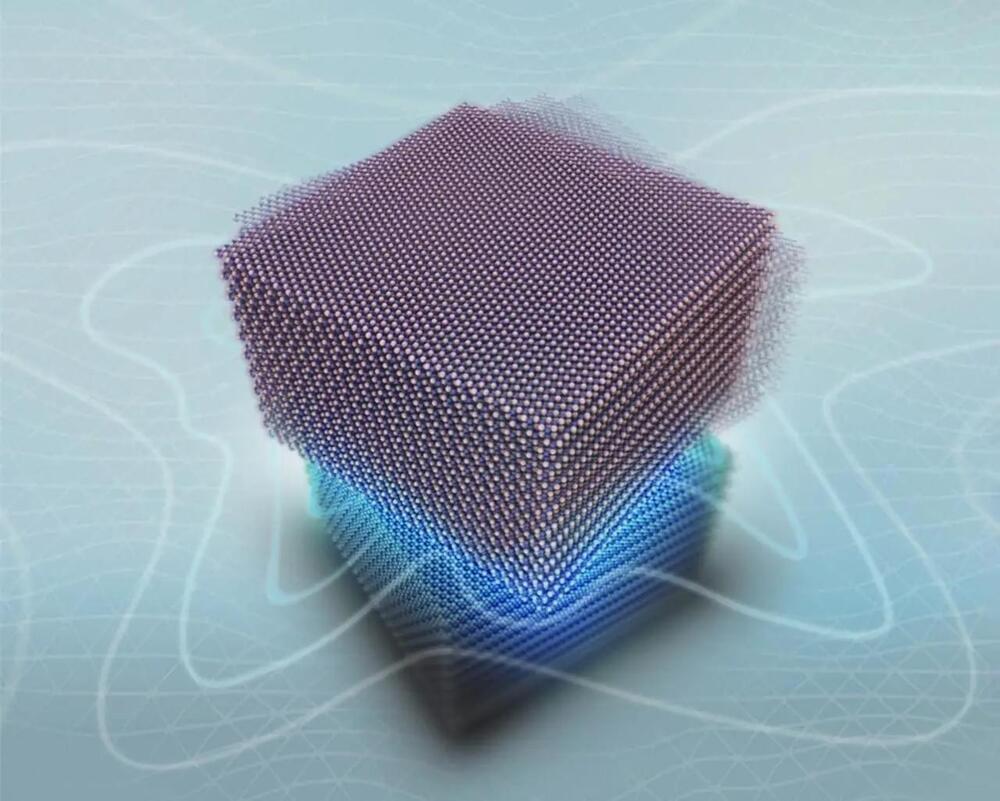
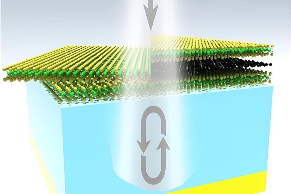
Scientists at The University of Manchester’s National Graphene Institute have discovered new physics in graphite through the application of twistronics, revealing a 2.5-dimensional mixing of surface and bulk states. The research opens new possibilities in controlling electronic properties in both 2D and 3D materials.
Researchers in the National Graphene Institute (NGI) at The University of Manchester have revisited graphite, one of the most ancient materials on Earth, and discovered new physics that has eluded the field for decades.
The Complexity of Graphite.
Julia Greer discusses her life background and research career in this five-part oral history.
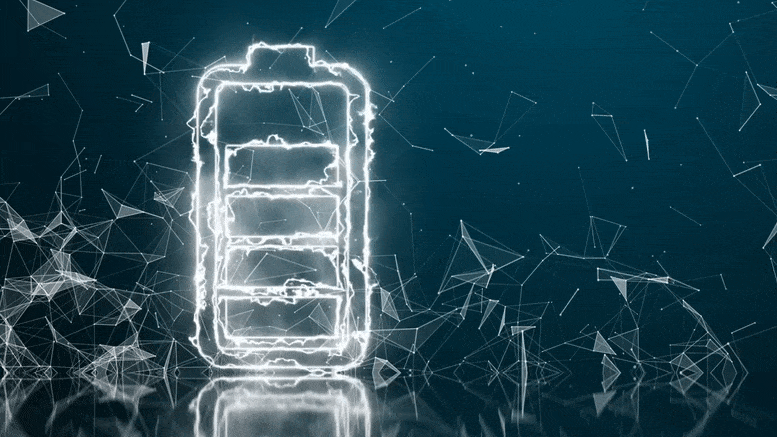
Metals traditionally serve as the active materials for the negative electrodes in batteries. However, there’s been a shift towards using redox-active organic molecules like quinone-and amine-based compounds as negative electrodes in rechargeable metal–air batteries, which feature oxygen-reducing positive electrodes.
Here, protons and hydroxide ions participate in the redox reactions. Such batteries exhibit high performance, close to the maximum capacity that is theoretically possible. Furthermore, using redox-active organic molecules in rechargeable air batteries overcomes problems associated with metals, including the formation of structures called ‘dendrites,’ which impact battery performance, and have negative environmental impact.
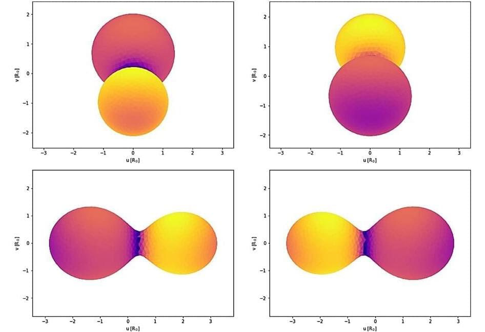
Using a private observatory, astronomers have performed the first photometric study of a peculiar W UMa-type binary known as CSS J003106.8+313347. Results of the study, published July 27 on the preprint server arXiv, shed more light on the properties of this system.
In general, W Ursae Majoris-type, or W UMa-type binaries (EWs) are eclipsing binaries with a short orbital period (below one day) and continuous light variation during a cycle. They are composed of two dwarf stars with similar temperature and luminosity, sharing a common envelope of material and are thus in contact with one another. Therefore, they are often dubbed “contact binaries.”
Located some 4,900 light years away, CSS J003106.8+313347 is an EW with an apparent magnitude of 14.73. The orbital period of the system is estimated to be approximately 0.344 days.
We can soon ascertain whether a room-temperature superconductor, with the potential to profoundly alter the world, has indeed been achieved.
Original samples of the alleged superconductor LK-99 could be available for validation studies as early as two weeks, Bloomberg.
A panel of experts convened by South Korea to examine the assertions made by the researchers released the update.
A University of Minnesota-led team has, for the first time, engineered an atomically thin material that can absorb nearly 100% of light at room temperature, a discovery that could improve a wide range of applications from optical communications to stealth technology. Their paper has been published in Nature Communications.
Materials that absorb nearly all of the incident light —meaning not a lot of light passes through or reflects off of them—are valuable for applications that involve detecting or controlling light.
“Optical communications are used in basically everything we do,” said Steven Koester, a professor in the College of Science and Engineering and a senior author of the paper. “The internet, for example, has optical detectors connecting fiber optic links. This research has the potential to allow these optical communications to be done at higher speeds and with greater efficiency.”
A study observes a triple protostar system with spiral arms of gas that feed material to baby stars and finds a new mechanism for multiple star formation.
A team of international researchers has discovered how three baby stars are being fed by spiral arms of gas in a triple protostar system. The team, led by Professor Jeong-Eun Lee from Seoul National University, used the powerful Atacama Large Millimeter/submillimeter Array (ALMA) telescopes to observe the system called IRAS 04239+2436, located about 460 light-years away from Earth.
They found that the gas around the three protostars contains sulfur monoxide (SO) molecules, which indicates the presence of shock waves caused by the complex… More.
Credit: ALMA (ESO/NAOJ/NRAO)
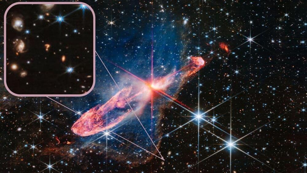
The James Webb Space Telescope continues to provide answers about the earliest days of the universe, but it’s also discovering more questions.
Question marks, to be precise. The James Webb Space Telescope (JWST) team at the European Space Agency (ESA) released an image on Wednesday (June 26) offering the most detailed look yet at two actively forming young stars located 1,470 light-years from Earth in the Vela Constellation. In the image, the stars, named Herbig-Haro 46/47, are surrounded by a disk of material that “feeds” the stars as they grow for millions of years.
While the superconducting properties and strong electron correlations observed in two-dimensional moiré superlattices do not persist in the three-dimensional bulk material, the teams’ observed Brown-Zak oscillations suggest that the bizarre characteristics of the 2D systems can be adopted even within thick graphite stacks. There may be a path toward reintroducing these more fascinating properties into bulk materials, Yankowitz says.
Moreover, the persistence of certain 2D behaviors in such thicker structures may explain some odd behaviors of graphite that have been observed as far back as the 1970s. “The behavior of graphite in a very strong magnetic field has been a bit of a mystery for a long time,” says Allan MacDonald, a physicist at the University of Texas at Austin, who did not participate in the work. “And these new papers may give a new handle on trying to understand what’s going on.”
This, Yankowitz says, opens up a new avenue of research in studying hybrid-dimensional materials. “Where this will lead right now is unclear, but it’s the foundation of understanding these new types of hybrid 2D-3D systems,” he says.