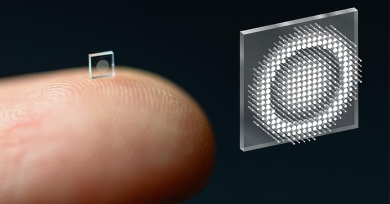
Researchers have created a salt-grain sized micro camera capable of taking images almost on par with a regular camera.
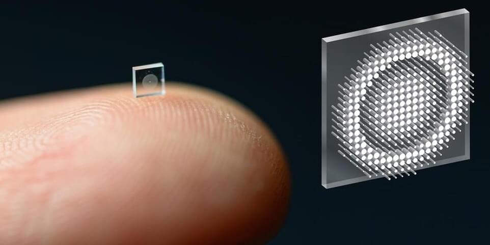
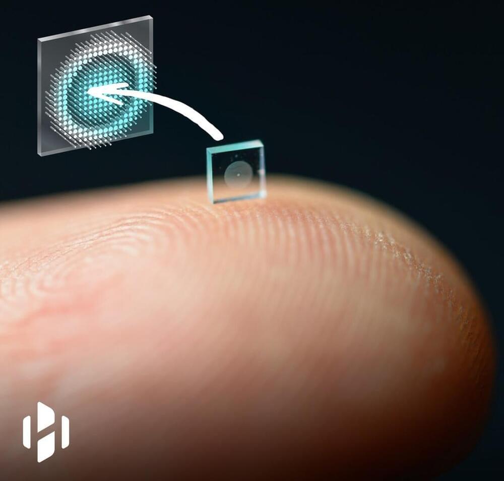
It is the highest resolution sensor of its type ever made.
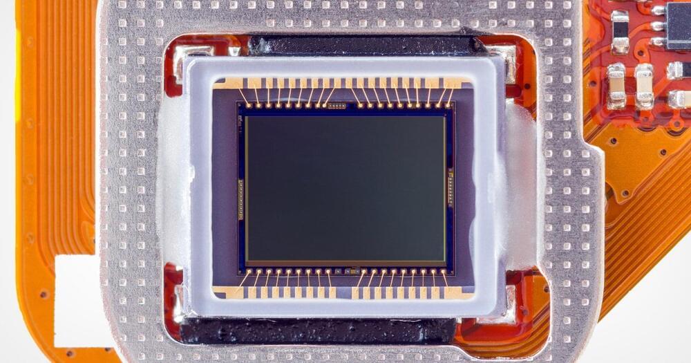
Canon has developed an image sensor that is capable of capturing high-quality color photography even in the dark. The company says that it will be able to shoot clear photos even in situations where nothing is visible to the naked eye.
In a report from Nikkei, Canon says that it has developed a new type of light-receiving element called a single photon avalanche diode (SPAD) and is implementing it on a CMOS sensor. SPAD photodetector technology on its own isn’t new, and has been in use since the 1970s. However, Canon has managed to create a sensor with 3.2 million pixels, which it says is more than three times the resolution of conventional SPADs and makes it the highest-resolution sensor of its type ever made.
The sensor is designed to replace, or at least provide an alternative to, infrared night vision cameras. Infrared is useful for recognizing shapes and providing sight in the dark, but is not capable of recognizing colors. On the flipside, cameras that can see color in the dark only do so by leveraging high ISOs, which can work to a certain point but eventually lead to extremely noisy images in levels of extreme darkness.

Months ago, before Windows 11 even shipped, beta users were complaining that Windows 11 was slowing their random write speeds on NVMe SSD by more than half.
Now, three months later and two months after the launch of the OS, it appears the issue is persisting.
Recent CrystalDiskMark benchmarks of the Samsung 980 Pro SSD performed by PleasedPen25317 show a massive reduction in random write speeds for any partition with Windows 11 installed.
► Contact/Booking: [email protected].
Circa 2017
“Enabling early detection of diseases is one of the greatest opportunities we have for developing effective treatments,” Esfandyarpour said. “Maybe $1 in the U.S. doesn’t count that much, but somewhere in the developing world, it’s a lot of money.”
A two-part system
A combination of microfluidics, electronics and inkjet printing technology, the lab-on-a-chip is a two-part system: A clear silicone microfluidic chamber for housing cells sits on top of a reusable electronic strip.

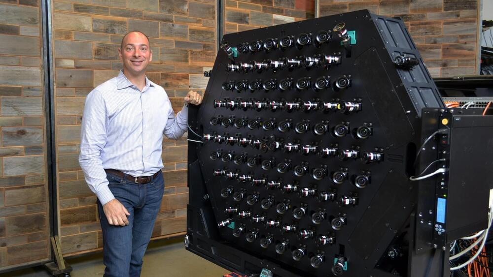
Lytro’s Immerge light-field camera is meant for professional high-end VR productions. It may be a beast of a rig, but it’s capable of capturing some of the best looking volumetric video that I’ve had my eyes on yet. The company has revealed a major update to the camera, the Immerge 2.0, which, through a few smart tweaks, makes for much more efficient production and higher quality output.
Light-field specialist Lytro, which picked up a $60 million Series D investment earlier this year, is making impressive strides in its light-field capture and playback technology. The company is approaching light-field from both live-action and synthetic ends; last month Lytro announced Volume Tracer, a software which generates light-fields from pre-rendered CG content, enabling ultra-high fidelity VR imagery that retains immersive 6DOF viewing.
Immerge 2.0
On the live-action end, the company has been building a high-end light-field camera which they call Immerge. Designed for high-end productions, the camera is actually a huge array of individual lenses which all work in unison to capture light-fields of the real world.