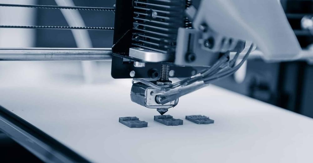
3D printed ICs overcome semiconductor shortage and reinforce supply chains, leading to cheaper production costs, faster prototyping, and faster time to market.
As the size of microchip packages shrinks, semiconductor manufacturers are under pressure to improve lithography capabilities. For more than two decades, researchers have been working on 3D printed integrated circuits. Earlier attempts at 3D printing electronics used the proper technique but failed to reach the required levels of conductivity for a PCB, leaving complicated electrical circuits unusable. Over time though, these printing tools have gradually improved feature size resolution, yield, and variability in production.
● A broad variety of materials may be used to produce an assortment of printed electronics, including conductors, semiconductors, dielectrics, resistors, and other components. ● As has been the case in other areas, additive manufacturing is expected to result in more innovative products, lower costs, and faster production runs.
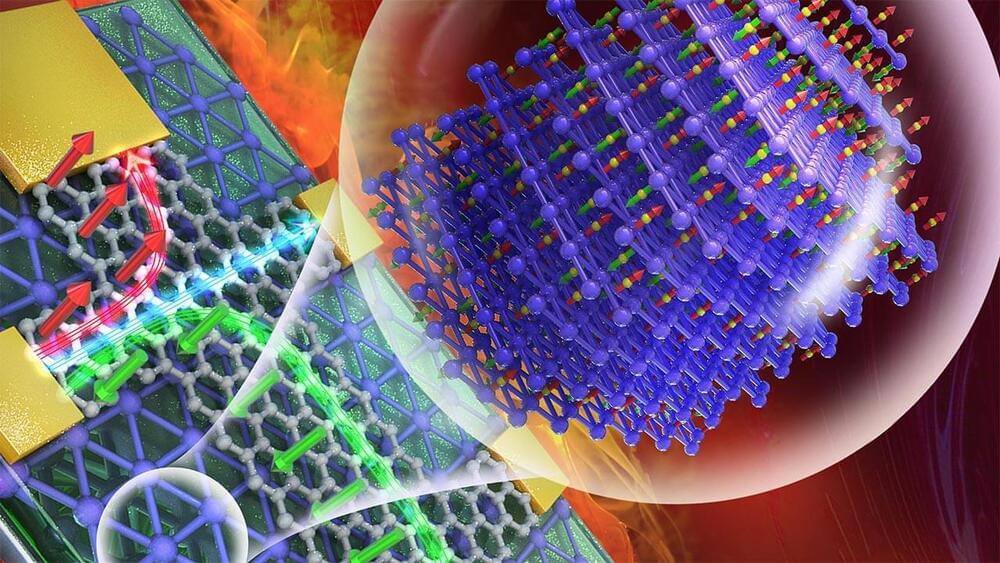
Design also poised to save space, retain memory in event of power loss. A new spin on one of the 20th century’s smallest but grandest inventions, the transistor, could help feed the world’s ever-growing appetite for digital memory while slicing up to 5% of the energy from its power-hungry diet.
A new spin on one of the 20th century’s smallest but grandest inventions, the transistor, could help feed the world’s ever-growing appetite for digital memory while slicing up to 5% of the energy from its power-hungry diet.
Following years of innovations from the University of Nebraska–Lincoln’s Christian Binek and University at Buffalos Jonathan Bird and Keke He, the physicists recently teamed up to craft the first magneto-electric transistor.
Along with curbing the energy consumption of any microelectronics that incorporate it, the team’s design could reduce the number of transistors needed to store certain data by as much as 75%, said Nebraska physicist Peter Dowben, leading to smaller devices. It could also lend those microelectronics steel-trap memory that remembers exactly where its users leave off, even after being shut down or abruptly losing power.
One of the ways we can fully realize the potential of quantum computers is by basing them on both light and matter – this way, information can be stored and processed, but also travel at the speed of light.
Scientists have just taken a step closer to this goal, by successfully producing the largest hybrid particles of light and matter ever created.
These quasiparticles, known as Rydberg polaritons, were made with the help of a piece of stone containing cuprous oxide (Cu2O) crystals from an ancient deposit in Namibia, one of the few places in the world where cuprous oxide has been found in gemstone quality.
“Some pullback was expected, but the return to pre-COVID volumes was instantaneous rather than gradual,” he added. Other research firms including Canalys also report demand for Chromebooks has taken a sharp dive in recent months.
McCarron added: “Due to the decline in low-cost entry level shipments, the market average CPU selling price increased the most on-quarter in 23 years.” The average selling price is now at $168, up from $151, according to Mercury Research’s stats.
Combating Antibiotic-Resistant Bacteria — Dr. Erin Duffy, Ph.D., Chief of Research & Development, and Kevin Outterson, ESQ., Executive Director, CARB-X.
The Combating Antibiotic-Resistant Bacteria Biopharmaceutical Accelerator (CARB-X — https://carb-x.org/) is a global non-profit partnership accelerating antibacterial products to address drug-resistant bacteria, a leading cause of death around the world. 1.27 million deaths worldwide were attributed to resistant bacterial infections in 2019.
The CARB-X portfolio is the world’s most scientifically diverse, early development pipeline of new antibiotics, vaccines, rapid diagnostics and other products and represents the only global partnership that integrates solutions for the prevention, diagnosis and treatment of life-threatening bacterial infections, translating innovation from basic research to first-in-human clinical trials.
Dr. Erin Duffy, PhD., is Chief of Research & Development at CARB-X and she has two decades of drug-discovery and problem-solving experience in the antibiotic arena. She was previously with Rib-X Pharmaceuticals (now Melinta Therapeutics) where in increasing roles she helped to build and sustain a team of researchers that translated the company’s scientific platform into next-generation and novel antibiotics that target the ribosome. Her team’s most recent achievements include the de novo design and optimization of a completely new class of antibiotics, the pyrrolocytosines, which were supported in part by CARB-X. Prior to Rib-X, Erin was the Associate Director of Innovative Discovery Technologies at Achillion Pharmaceuticals, responsible for building the structure and computational teams and platform for their antiviral efforts. She began her industrial career at Pfizer Central Research, in Groton, Connecticut, where she joined a team of computational and structural drug designers in multiple therapeutic areas. Erin was trained formally at Yale University, where she became a physical-organic chemist focused on defining computationally how small molecules interact and react in the group of Professor William L. Jorgensen. She expanded her experience to large molecules under the mentorship of Professor Axel Brunger, whose group at Yale was transitioning to a mix of computational and laboratory structural biology.
Kevin Outterson, ESQ., is Executive Director of CARB-X and is a global thought leader on business models for antibiotic development and use. He is Professor of Law and N. Neil Pike Scholar of Health and Disability Law at Boston University School of Law, where he leads multi-disciplinary teams to solve global health issues. Professor Outterson is the Executive Director and Principal Investigator of CARB-X and a partner in DRIVE-AB (aka Driving Reinvestment In Research And Development And Responsible Antibiotic Use) a project composed of 15 public and 7 private partners from 12 countries that is funded by the Innovative Medicines Initiative (IMI) joint undertaking between the European Union and the European Pharmaceutical Industry Association (EFPIA). He also leads the Social Innovation on Drug Resistance program at Boston University.
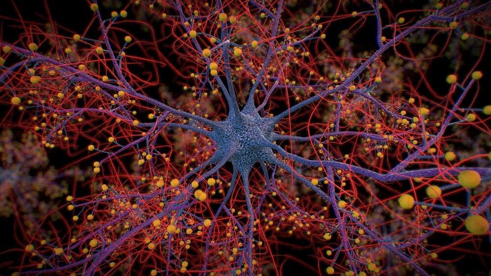
The brain is inarguably the single most important organ in the human body. It controls how we move, react, think and feel, and enables us to have complex emotions and memories. The brain is composed of approximately 86 billion neurons that form a complex network. These neurons receive, process, and transfer information using chemical and electrical signals.
Learning how neurons respond to different signals can further the understanding of cognition and development and improve the management of disorders of the brain. But experimentally studying neuronal networks is a complex and occasionally invasive procedure. Mathematical models provide a non-invasive means to accomplish the task of understanding neuronal networks, but most current models are either too computationally intensive, or they cannot adequately simulate the different types of complex neuronal responses. In a recent study, published in Nonlinear Theory and Its Applications, IEICE, a research team led by Prof. Tohru Ikeguchi of Tokyo University of Science, has analyzed some of the complex responses of neurons in a computationally simple neuron model, the Izhikevich neuron model.
“My laboratory is engaged in research on neuroscience and this study analyzes the basic mathematical properties of a neuron model. While we analyzed a single neuron model in this study, this model is often used in computational neuroscience, and not all of its properties have been clarified. Our study fills that gap,” explains Prof. Ikeguchi. The research team also comprised Mr. Yota Tsukamoto and Ph.D. student Ms. Honami Tsushima, also from Tokyo University of Science.
Scientists from Beijing set a new quantum secure direct communication (QSDC) world record of 102.2 km (64 miles), a massive leap over the previous record of 18 km (11 miles), according toThe Eurasian Times.
The research could eventually lead to a massive quantum communications network that would be virtually hacker-proof due to the nature of the technology.
The researchers, who published their findings in a paper in Nature, demonstrated transmission speeds of 0.54 bits per second, much slower than communications using classical computing devices. Still, this was fast enough for phone call and text message encryption over a distance of 30 km (19 miles).
Summary: The Izhikevich neuron model allows the simulation of both periodic and quasi-periodic responses in neurons at lower computational cost.
Source: Tokyo University of Science.
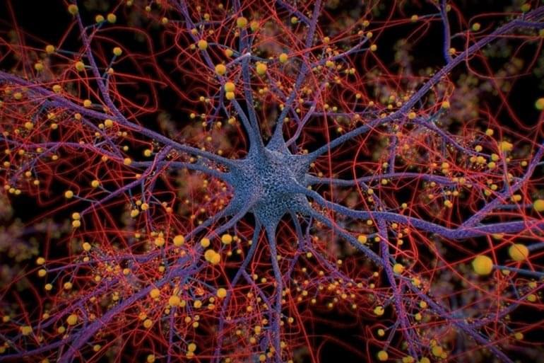
The brain is inarguably the single most important organ in the human body. It controls how we move, react, think and feel, and enables us to have complex emotions and memories. The brain is composed of approximately 86 billion neurons that form a complex network. These neurons receive, process, and transfer information using chemical and electrical signals.


