Menu

Blog

Archive for the ‘computing’ category: Page 544

May 7, 2020

A Discovery That Long Eluded Physicists: Superconductivity to the Edge

Posted by in categories: computing, quantum physics

Princeton researchers detect a supercurrent a current flowing without energy loss at the edge of a superconductor with a topological twist.

A discovery that long eluded physicists has been detected in a laboratory at Princeton. A team of physicists detected superconducting currents — the flow of electrons without wasting energy — along the exterior edge of a superconducting material. The finding was published May 1 in the journal Science.

The superconductor that the researchers studied is also a topological semi-metal, a material that comes with its own unusual electronic properties. The finding suggests ways to unlock a new era of “topological superconductivity” that could have value for quantum computing.

May 5, 2020

Researchers demonstrate pattern recognition using magnonic holographic memory device

Posted by in categories: computing, materials

Circa 2015


Researchers at the University of California, Riverside Bourns College of Engineering and the Russian Academy of Sciences have successfully demonstrated pattern recognition using a magnonic holographic memory device, a development that could greatly improve speech and image recognition hardware.

Pattern recognition focuses on finding patterns and regularities in data. The uniqueness of the demonstrated work is that the input patterns are encoded into the phases of the input spin waves.

Continue reading “Researchers demonstrate pattern recognition using magnonic holographic memory device” »

May 5, 2020

Scientists produce a magnetic nanocrystal with many potential applications

Posted by in categories: chemistry, computing, nanotechnology, quantum physics

Spinels are oxides with chemical formulas of the type AB2O4, where A is a divalent metal cation (positive ion), B is a trivalent metal cation, and O is oxygen. Spinels are valued for their beauty, which derives from the molecules’ spatial configurations, but spinels in which the trivalent cation B consists of the element chrome (Cr) are interesting for a reason that has nothing to do with aesthetics: They have magnetic properties with an abundance of potential technological applications, including gas sensors, drug carriers, data storage media, and components of telecommunications systems.

A study by Brazilian and Indian researchers investigated a peculiar kind of spinel: zinc-doped manganese chromite. Nanoparticles of this material, described by the formula Mn0.5 Zn0.5 Cr2O4 [where manganese (Mn) and zinc (Zn) compose the A-site divalent cation], were synthesized in the laboratory and characterized by calculations based on density functional theory (DFT), a method derived from that is used in solid-state physics and chemistry to resolve complex crystal structures.

The material’s structural, electronic, vibrational and were determined by X-ray diffraction, neutron diffraction, X-ray photoelectron spectroscopy and Raman spectroscopy. A report of the study has been published in the Journal of Magnetism and Magnetic Materials with the title “Structural, electronic, vibrational and magnetic properties of Zn2+ substituted MnCr2O4 nanoparticles.”

May 5, 2020

Towards fungal computer

Posted by in categories: chemistry, computing

Circa 2018


We propose that fungi Basidiomycetes can be used as computing devices: information is represented by spikes of electrical activity, a computation is implemented in a mycelium network and an interface is realized via fruit bodies. In a series of scoping experiments, we demonstrate that electrical activity recorded on fruits might act as a reliable indicator of the fungi’s response to thermal and chemical stimulation. A stimulation of a fruit is reflected in changes of electrical activity of other fruits of a cluster, i.e. there is distant information transfer between fungal fruit bodies. In an automaton model of a fungal computer, we show how to implement computation with fungi and demonstrate that a structure of logical functions computed is determined by mycelium geometry.

The fungi are the largest, widely distributed and oldest group of living organisms [1]. The smallest fungi are microscopic single cells. The largest mycelium belongs to Armillaria bulbosa, which occupies 15 hectares and weights 10 tons [2], and the largest fruit body belongs to Fomitiporia ellipsoidea, which at 20 years old is 11 m long, 80 cm wide, 5 cm thick and has an estimated weight of nearly half-a-ton [3]. During the last decade, we produced nearly 40 prototypes of sensing and computing devices from the slime mould Physarum polycephalum [4], including the shortest path finders, computational geometry processors, hybrid electronic devices, see the compilation of the latest results in [5].

May 5, 2020

The subatomic age: Asia’s quantum computing arms race

Posted by in categories: computing, quantum physics

Huawei and Alibaba among tech giants pouring money into development.

PETER GUEST, Nikkei staff writer May 05, 2020 13:05 JST.

May 4, 2020

Implementation of PPI with Nano Amorphous Oxide Semiconductor Devices for Medical Applications

Posted by in categories: biotech/medical, computing, neuroscience

Electronic devices which mimic the functionality of biological synapses are a large step to replicate the human brain for neuromorphic computing and for numerous medical research investigations. One of the representative synaptic behaviors is paired-pulse facilitation (PPF). It has been widely investigated because it is regarded to be related to biological memory. However, plasticity behavior is only part of the human brain memory behavior.

Here, we present a phenomenon which is opposite to PPF, i.e., paired-pulse inhibition (PPI), in nano oxide devices for the first time. The research here suggests that rather than being enhanced, the phenomena of memory loss would also be possessed by such electronic devices. The device physics mechanism behind memory loss behavior was investigated. This mechanism is sustained by historical memory and degradation manufactured by device trauma to regulate characteristically stimulated origins of artificial transmission behaviors.

Under the trauma of a memory device, both the signal amplitude and signal time stimulated by a pulse are lower than the first signal stimulated by a previous pulse in the PPF, representing a new scenario in the struggle for memory. In this way, more typical human brain behaviors could be simulated, including the effect of age on latency and error generation, cerebellar infarct, trauma and memory loss pharmacological actions (such as those caused by hyoscines and nitrazepam).

May 4, 2020

To make an atom-sized machine, you need a quantum mechanic

Posted by in categories: computing, nanotechnology, particle physics, quantum physics

Here’s a new chapter in the story of the miniaturisation of machines: researchers in a laboratory in Singapore have shown that a single atom can function as either an engine or a fridge. Such a device could be engineered into future computers and fuel cells to control energy flows.

“Think about how your computer or laptop has a lot of things inside it that heat up. Today you cool that with a fan that blows air. In nanomachines or quantum computers, small devices that do cooling could be something useful,” says Dario Poletti from the Singapore University of Technology and Design (SUTD).

This work gives new insight into the mechanics of such devices. The work is a collaboration involving researchers at the Centre for Quantum Technologies (CQT) and Department of Physics at the National University of Singapore (NUS), SUTD and at the University of Augsburg in Germany. The results were published in the peer-reviewed journal npj Quantum Information on 1 May.

May 2, 2020

Smart chips for space

Posted by in categories: computing, space

Tiny integrated circuits destined for space missions, etched onto a single wafer of silicon, examined under a magnifier.

To save money on the high cost of fabrication, various chips designed by different companies and destined for multiple ESA projects are crammed onto the same silicon wafers, etched into place at specialised semiconductor manufacturing plants or ‘fabs’.

Once manufactured, the chips, still on the wafer, are tested. The wafers are then chopped up. They become ready for use when placed inside protective packages – just like standard terrestrial microprocessors – and undergo final quality tests.

May 2, 2020

In search of the lighting material of the future

Posted by in categories: computing, mobile phones

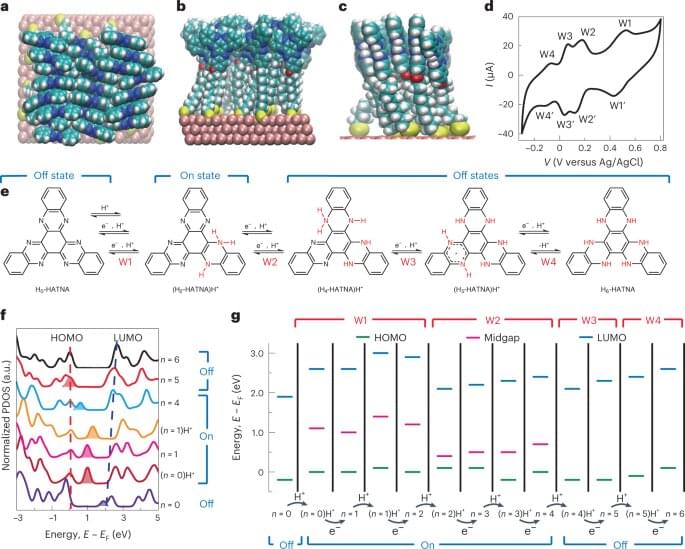
At the Paul Scherrer Institute PSI, researchers have gained insights into a promising material for organic light-emitting diodes (OLEDs). The substance enables high light yields and would be inexpensive to produce on a large scale—that means it is practically made for use in large-area room lighting. Researchers have been searching for such materials for a long time. The newly generated understanding will facilitate the rapid and cost-efficient development of new lighting appliances in the future. The study appears today in the journal Nature Communications.

The compound is a yellowish solid. If you dissolve it in a liquid or place a of it on an electrode and then apply an , it gives off an intense green glow. The reason: The molecules absorb the energy supplied to them and gradually emit it again in the form of light. This process is called electroluminescence. Light-emitting diodes are based on this principle.

This green luminescent substance is a hot candidate for producing OLEDs, -emitting diodes. For about three years now, OLEDs have been found in the displays of smartphones, for example. In the meantime, the first flexible television screens with these materials have also come onto the market.

May 2, 2020

Researchers see path to quantum computing at room temperature

Posted by in categories: computing, military, quantum physics

Army researchers predict quantum computer circuits that will no longer need extremely cold temperatures to function could become a reality after about a decade.

For years, solid-state quantum technology that operates at room temperature seemed remote. While the application of transparent crystals with had emerged as the most likely route to this milestone, the plausibility of such a system always remained in question.

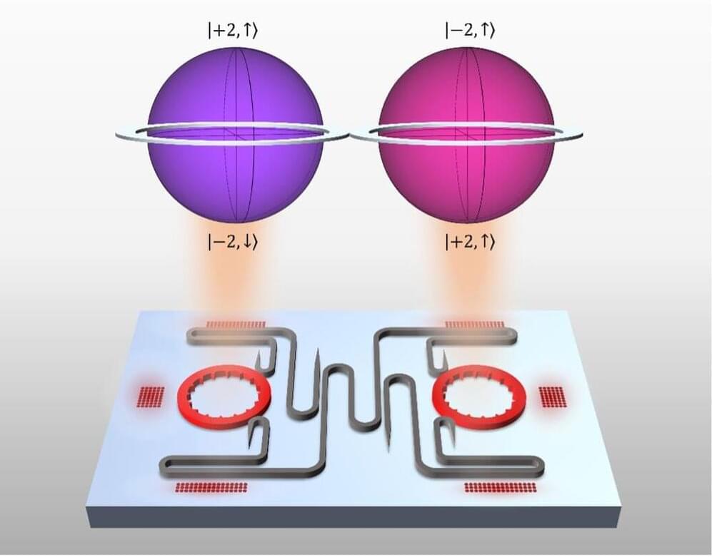
Now, Army scientists have officially confirmed the validity of this approach. Dr. Kurt Jacobs, of the U.S. Army Combat Capabilities Development Command’s Army Research Laboratory, working alongside Dr. Mikkel Heuck and Prof. Dirk Englund, of the Massachusetts Institute of Technology, became the first to demonstrate the feasibility of a quantum logic gate comprised of and optical crystals.