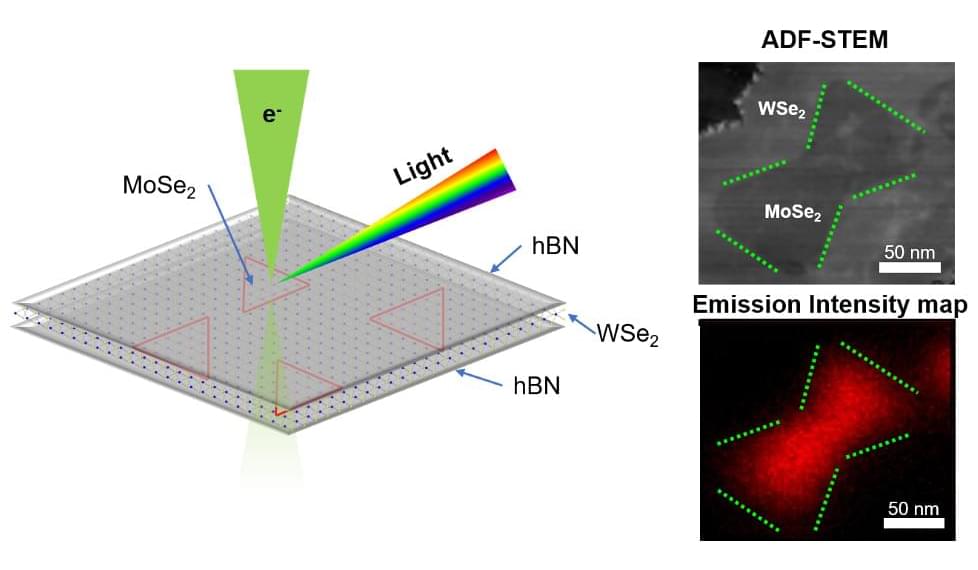
RuO2 has been established as the benchmark catalyst for the oxygen evolution reaction (OER). However, the low precious metal content compared to other OER industrial catalysts like RuO2, Pt/C, and IrO2 makes a hybrid heterosurface of RuO2 and F-doped graphene (RuO2@FGr) an excellent catalyst with a high current density. Moreover, the advantage of graphene support increases stability. We investigated the mechanism of the OER on RuO2@FGr using density functional theory (DFT) and the computational hydrogen electrode model (CHEM). In CHEM, the adsorption energy of the reactive intermediates is considered for the reduction potential calculation. This is followed by free energy calculation and, eventually, overpotential calculation using standard or reversible hydrogen electrodes (SHE/RHE). Computational OER activity calculated in the gas phase using density functional theory (DFT) cannot explain the contribution of the condensed phase, water organization energy, the kinetics of the elementary steps, and electrochemical contribution. The current study will address the issue by implementing an implicit solvation model and the electrostatic contribution by considering the charge extrapolation model. We used molecular RuO2 to mimic the exact experimental weight percentage. Fluorine intercalation doping improves the binding of oxygen-based intermediate species to the reactive surface due to a shift in the d-band center toward the Fermi level. The graphene sheet behaves as a conductor after fluorine doping, and the electron density contribution near the Fermi level is clearly distinguished from the projected density of states (PDOS). Using the implicit solvation model with altered parameters, we find improvements in the reaction barrier for hydroperoxo formation. An overpotential of 0.40 V vs RHE is obtained for the cavity shape parameter and charge density cutoff parameter of 0.8 and 0.0035 Å–3. For completion, we implement the constant potential model (CPM) to extrapolate our results calculated at the nonzero potential environment to 0.0 V potential. The mean energy path computed using the climbing image nudged elastic band provides the activation and reaction energy, and the values are extrapolated to 0.0 V RHE using the CPM correction. Implementing both thermochemical and electrochemical corrections simultaneously, we can find a reasonable overpotential of the studied catalytic reaction.
Category: computing – Page 220
Relying on sub-wavelength nanostructures, metasurfaces have been shown as promising candidates for replacing conventional free-space optical components by arbitrarily manipulating the amplitude, phase, and polarization of optical wavefronts in certain applications1,2,3. In recent years, the scope of their applications has been expanded towards complete spatio-temporal control through the introduction of active metasurfaces. These developments open up exciting new possibilities for dynamic holography4, faster spatial light modulators5, and fast optical beam steering for LiDAR6. Large efforts have been channeled into various modulation mechanisms7. Microelectromechanical and nanoelectromechanical systems (MEMS and NEMS)8,9,10,11 have the advantages of low-cost and CMOS-compatibility, but the speed is limited up to MHz. Phase-change materials12,13,14 have fast, drastic, and non-volatile refractive index change, but lack continuous refractive index tuning and have a limited number of cycles constraining applicability to reconfigurable devices. Through molecule reorientation, liquid crystal can have index modulation over 10%, while under relatively low applied voltages Tunable liquid crystal metasurfaces, U.S. patent number 10,665,953 [Application Number 16/505,687]15. Techniques of liquid crystal integration have also advanced after decades of development. However, the tuning speeds are limited to kHz range16. Thermal-optic effects can induce relatively large refractive index changes17,18, but the speed is inherently limited and the on-chip thermal management can be challenging. The co-integration of transparent conductive oxide and metallic plasmonic structures5,6 has been demonstrated in epsilon-near-zero (ENZ) regime to control the wavefront of reflected light, but the low reflection amplitude induced by the optical loss of the materials and the ENZ regime is unavoidable.
In modern photonics, a multitude of technologies for tunable optics and frequency conversion19,20 are realized with nonlinear materials that have low loss and a strong χ effect, such as lithium niobate21,22, aluminum nitride23, and organic electro-optic (OEO) materials24. Their ultrafast responses make it possible to use RF or millimeter-wave control25. Developments in computational chemistry have also led to artificially engineered organic molecules that have record-high nonlinear coefficients with long-term and high-temperature stability26,27. However, their potential in modifying free-space light has been relatively unexplored until recently. Several OEO material-hybrid designs have demonstrated improved tunability of metasurfaces28,29,30. Utilizing dielectric resonant structures and RF-compatible coplanar waveguides, a free-space silicon-organic modulator has recently accomplished GHz modulation speed31. However, all demonstrations to date require high operating voltages ± 60V, due to low resonance tuning capability (frequency shift / voltage), which hinders their integration with electronic chips.
In this work, we propose combining high-Q metasurfaces based on slot-mode resonances with the unique nano-fabrication techniques enabled by OEO materials, which drastically reduces the operating voltage. The low voltage is mainly achieved from the ability to place the electrodes in close proximity to each other while hosting high-Q modes in between and the large overlap of the optical and RF fields in OEO materials. In the following sections, we first provide the design concepts and considerations for achieving a reduced operating voltage. Next, we numerically demonstrate the advantage of a particular selected mode compared to other supported modes in the structure. Finally, we experimentally realize our concepts and characterize the performance of the electro-optic metasurface.
Musk said that the first human patient implanted with a Neuralink chip last month “is able to… move the mouse around the screen just by thinking.”
How Does The Neutral Atom Approach Compare
The neutral atom approach is a well-known and extensively investigated approach to quantum computing. The approach offers numerous advantages, especially in terms of scalability, expense, error mitigation, error correction, coherence, and simplicity.
Neutral atom quantum computing utilizes individual atoms, typically alkali atoms like rubidium or cesium, suspended and isolated in a vacuum and manipulated using precisely targeted laser beams. These atoms are not ionized, meaning they retain all their electrons and do not carry an electric charge, which distinguishes them from trapped ion approaches. The quantum states of these neutral atoms, such as their energy levels or the orientation of their spins, serve as the basis for qubits. By employing optical tweezers—focused laser beams that trap and hold the atoms in place—arrays of atoms can be arranged in customizable patterns, allowing for the encoding and manipulation of quantum information.
Elon Musk announced this week that his company’s brain implant has allowed a person to move a computer mouse with their mind.
Relying on sub-wavelength nanostructures, metasurfaces have been shown as promising candidates for replacing conventional free-space optical components by arbitrarily manipulating the amplitude, phase, and polarization of optical wavefronts in certain applications1,2,3. In recent years, the scope of their applications has been expanded towards complete spatio-temporal control through the introduction of active metasurfaces. These developments open up exciting new possibilities for dynamic holography4, faster spatial light modulators5, and fast optical beam steering for LiDAR6. Large efforts have been channeled into various modulation mechanisms7. Microelectromechanical and nanoelectromechanical systems (MEMS and NEMS)8,9,10,11 have the advantages of low-cost and CMOS-compatibility, but the speed is limited up to MHz. Phase-change materials12,13,14 have fast, drastic, and non-volatile refractive index change, but lack continuous refractive index tuning and have a limited number of cycles constraining applicability to reconfigurable devices. Through molecule reorientation, liquid crystal can have index modulation over 10%, while under relatively low applied voltages Tunable liquid crystal metasurfaces, U.S. patent number 10,665,953 [Application Number 16/505,687]15. Techniques of liquid crystal integration have also advanced after decades of development. However, the tuning speeds are limited to kHz range16. Thermal-optic effects can induce relatively large refractive index changes17,18, but the speed is inherently limited and the on-chip thermal management can be challenging. The co-integration of transparent conductive oxide and metallic plasmonic structures5,6 has been demonstrated in epsilon-near-zero (ENZ) regime to control the wavefront of reflected light, but the low reflection amplitude induced by the optical loss of the materials and the ENZ regime is unavoidable.
In modern photonics, a multitude of technologies for tunable optics and frequency conversion19,20 are realized with nonlinear materials that have low loss and a strong χ effect, such as lithium niobate21,22, aluminum nitride23, and organic electro-optic (OEO) materials24. Their ultrafast responses make it possible to use RF or millimeter-wave control25. Developments in computational chemistry have also led to artificially engineered organic molecules that have record-high nonlinear coefficients with long-term and high-temperature stability26,27. However, their potential in modifying free-space light has been relatively unexplored until recently. Several OEO material-hybrid designs have demonstrated improved tunability of metasurfaces28,29,30. Utilizing dielectric resonant structures and RF-compatible coplanar waveguides, a free-space silicon-organic modulator has recently accomplished GHz modulation speed31. However, all demonstrations to date require high operating voltages ± 60V, due to low resonance tuning capability (frequency shift / voltage), which hinders their integration with electronic chips.
In this work, we propose combining high-Q metasurfaces based on slot-mode resonances with the unique nano-fabrication techniques enabled by OEO materials, which drastically reduces the operating voltage. The low voltage is mainly achieved from the ability to place the electrodes in close proximity to each other while hosting high-Q modes in between and the large overlap of the optical and RF fields in OEO materials. In the following sections, we first provide the design concepts and considerations for achieving a reduced operating voltage. Next, we numerically demonstrate the advantage of a particular selected mode compared to other supported modes in the structure. Finally, we experimentally realize our concepts and characterize the performance of the electro-optic metasurface.
MIT researchers used ultrathin van der Waals materials to create an electron magnet that can be switched at room temperature. This type of magnet could be used to build magnetic processors or memories that would consume far less energy than silicon devices.
The Quantum Insider (TQI) is the leading online resource dedicated exclusively to Quantum Computing.
Neuralink’s first human patient able to use mouse…:
Elon Musk is the visionary behind Neuralink. He announced that the first human recipient of the company’s brain chip implant has fully recovered. The individual has demonstrated the ability to use a computer mouse solely through thoughts. Watch this video for all details.
#Neuralink #ElonMusk #WION
About Channel:
WION The World is One News examines global issues with in-depth analysis. We provide much more than the news of the day. Our aim is to empower people to explore their world. With our Global headquarters in New Delhi, we bring you news on the hour, by the hour. We deliver information that is not biased. We are journalists who are neutral to the core and non-partisan when it comes to world politics. People are tired of biased reportage and we stand for a globalized united world. So for us, the World is truly One.
Creating a quantum computer powerful enough to tackle problems we cannot solve with current computers remains a big challenge for quantum physicists. A well-functioning quantum simulator – a specific type of quantum computer – could lead to new discoveries about how the world works at the smallest scales. Quantum scientist Natalia Chepiga from Delft University of Technology has developed a guide on how to upgrade these machines so that they can simulate even more complex quantum systems. The study is now published in Physical Review Letters.
“Creating useful quantum computers and quantum simulators is one of the most important and debated topics in quantum science today, with the potential to revolutionize society,” says researcher Natalia Chepiga. Quantum simulators are a type of quantum computer, Chepiga explains: “Quantum simulators are meant to address open problems of quantum physics to further push our understanding of nature. Quantum computers will have wide applications in various areas of social life, for example in finances, encryption, and data storage.”
Steering Wheel