A newly designed structure exhibits the largest-recorded emissivity–absorptivity difference, a property that could prove useful in energy-harvesting and cloaking devices.
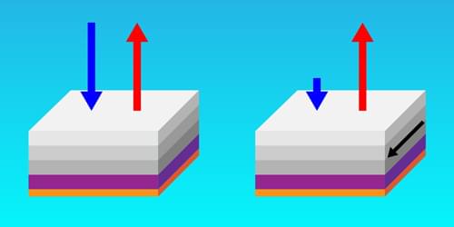
Hot objects glow. From the warmth of a stovetop to the invisible heat radiating from a building’s roof, thermal radiation flows outward. But it also flows inward in a reciprocal manner. This means that at thermal equilibrium, an object’s ability to thermally emit light in one direction, described as emissivity, is equal to its ability to absorb the same light coming in from the other direction, known as absorptivity. But what if this rule could be violated?
In a new study, Zhenong Zhang and colleagues from Pennsylvania State University demonstrate this exciting possibility [1]. The researchers apply an external magnetic field to a layered material, creating a system that breaks Lorentz reciprocity—a common symmetry that relates electromagnetic inputs and outputs. They then show that this nonreciprocal system exhibits much higher emissivity than absorptivity in the same direction. The observed difference between emissivity and absorptivity is twice that observed in previous experiments, thus setting a new benchmark in the field. These results pave the way for future technologies such as thermal diodes, radiative heat engines, and infrared camouflage.