Toggle light / dark theme

Intel debuts new chip focused on addressing quantum computing’s wiring bottleneck.

Intel’s millikelvin quantum research control chip, code-named Pando Tree, establishes Intel as the first semiconductor manufacturer to demonstrate the distribution of cryogenic silicon spin qubit control electronics…


Sushil Subramanian is a research scientist at Intel where he works on integrated circuits and systems for qubit control in quantum computers. Co-author Stefano Pellerano is a senior principal engineer and lab director of the RF and Mixed-Signal Circuits Lab where he leads the research and development effort on cryogenic electronics for qubit control.

A trio of physicists, two with Uniwersytet Jagielloński in Poland and one with Swinburne University of Technology in Australia, are proposing the use of temporal printed circuit boards made using time crystals as a way to solve error problems on quantum computers. Krzysztof Giergiel, Krzysztof Sacha and Peter Hannaford have written a paper describing their ideas, which is currently available on the arXiv preprint server.

A collaboration of Professor Szameit’s research group at the University of Rostock with researchers from the Albert-Ludwigs-Universität Freiburg has succeeded in stabilizing the interference of two photons in optical chips with the concept of topologically protected wave propagation. The research results are published in Science.

In today’s semiconductor manufacturing industry, the most advanced chips are produced at 7 nm and below where there is little room for error. Despite the difficulty and unrelenting pressures found in this microworld, engineers and scientists remain undeterred in their pursuit of cutting-edge processes, techniques or materials that push the boundaries of Moore’s Law. Through endless experimentation at the nanoscale level, designers and researchers seek to uncover minute improvements that have the potential to translate into millions—if not billions—of dollars in revenue for chipmakers.

The emergence of carbon nanotubes (CNTs) as a compelling alternative material to address inefficiencies in extreme ultraviolet (EUV) lithography has the potential to be one of those innovations. However, contemporary production methods create CNTs that fall short of expectations. To realize the full potential of CNTs requires a new production method that significantly improves their quality. Only then can they help the semiconductor industry deliver on the insatiable demands for advanced chips.

Before exploring the production methods behind creating CNTs, one must first understand why they are so crucial in the semiconductor industry.

In the race to develop practical quantum computers, a team of researchers has achieved a significant milestone by demonstrating a new method for manipulating quantum information. This breakthrough, published in the journal Nature Communications, could lead to faster and more efficient quantum computing by harnessing the power of customizable “nonlinearities” in superconducting circuits.

Quantum computers promise to revolutionize computing by leveraging the principles of quantum mechanics to perform complex calculations that are impossible for classical computers. However, one of the main challenges in building quantum computers is the difficulty in manipulating and controlling quantum information, known as qubits.

The researchers, led by Axel M. Eriksson and Simone Gasparinetti from Chalmers University of Technology in Sweden, have developed a novel approach that allows for greater control over qubits by using a special type of superconducting circuit called a SNAIL (Superconducting Nonlinear Asymmetric Inductive eLement) resonator.

Spintronics relies on the transport of spin currents for computing and communication applications. New device designs would be possible if this spin transport could be carried out by both electrons and magnetic waves called magnons. But spin transport via magnons typically requires electrically insulating magnets—materials that cannot be easily integrated with silicon electronics. A way to bypass that requirement has now been found by Matthias Althammer at the Bavarian Academy of Sciences and Humanities in Germany and his colleagues [1]. The researchers say that this finding could have important implications for both spintronic applications and fundamental research on spin transport.

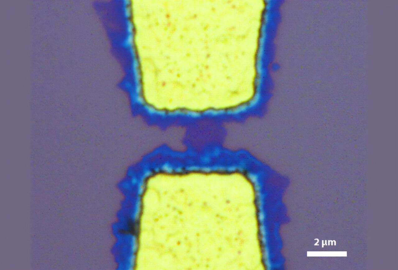
To demonstrate their concept, Althammer and his colleagues placed two magnetic, metallic strips—each hosting coupled electrons and magnons—on a nonmagnetic, insulating substrate. In the first strip, the researchers converted electron charge currents to electron spin currents. These spin currents were transferred first to the magnons in the same strip, then across the substrate to the magnons in the second strip, and finally to the electrons in the second strip. The researchers detected this spin transport by converting the electron spin currents in the second strip to charge currents.

Althammer and his colleagues studied how the spin transport between the two strips depended on temperature and strip separation. These measurements suggested that the transport was achieved via a magnetic dipole–dipole interaction between the strips. But the researchers could not rule out the possibility that it partly or mainly occurred via crystal vibrations in the substrate. Solving this open problem, which the researchers plan to do in upcoming work, will help in optimizing devices based on this principle.