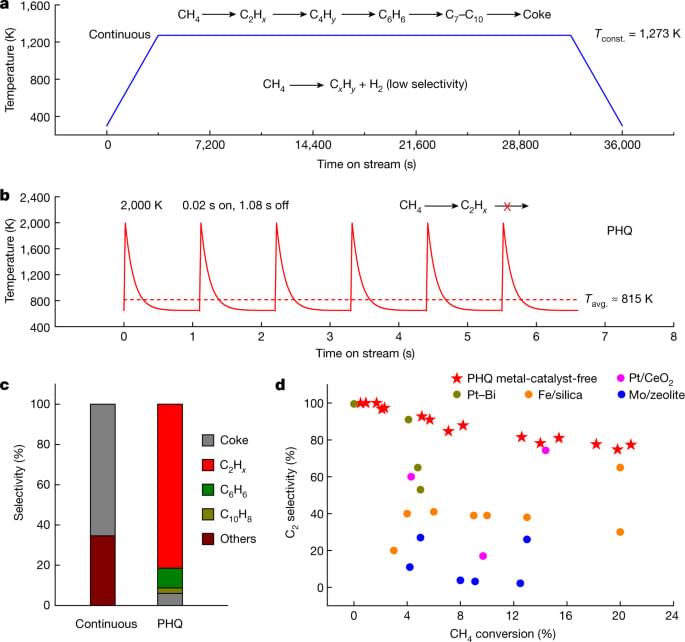
By using a programmable electric current to allow rapid pulsed heating and quenching, a non-equilibrium, continuous synthesis technique shows improved performance in thermochemical reactions, as well as lower energy costs.
During a high-level talk on NASA’s objectives for human space exploration, we got an early glimpse of what a 30 day crewed mission to the surface of Mars could eventually look like.
It’s an exciting prospect that, while many years if not decades away, shows the agency’s commitment to fulfilling humanity’s dreams of setting foot on the Red Planet for the first time in history.
NASA director of space architectures Kurt “Spuds” Vogel outlined what such a mission could entail. The agency is envisioning a habitat spacecraft to make the months long journey there, which uses a hybrid rocket stage that combines chemical and electric propulsion.
Scientists are attempting to map the wiring of the nearly 100 billion neurons in the human brain. Are we close to uncovering the mysteries of the mind or are we only at the beginning of a new frontier?
PARTICIPANTS: Deanna Barch, Jeff Lichtman, Nim Tottenham, David Van Essen.
MODERATOR: John Hockenberry.
Original program date: JUNE 4, 2017
WATCH THE TRAILER: https://youtu.be/lX5S_1bXUhw.
WATCH THE LIVE Q&A W/ JEFF LICHTMAN: https://youtu.be/h14hcBrqGSg.
Imagine navigating the globe with a map that only sketched out the continents. That’s pretty much how neuroscientists have been operating for decades. But one of the most ambitious programs in all of neuroscience, the Human Connectome Project, has just yielded a “network map” that is shedding light on the intricate connectivity in the brain. Join leading neuroscientists and psychologists as they explore how the connectome promises to revolutionize treatments for psychiatric and neurological disorders, answer profound questions regarding the electrochemical roots of memory and behavior, and clarify the link between our upbringing and brain development.
MORE INFO ABOUT THE PROGRAM AND PARTICIPANTS: https://www.worldsciencefestival.com/programs/wired-life-mapping-connectome/
This program is part of the Big Ideas Series, made possible with support from the John Templeton Foundation.
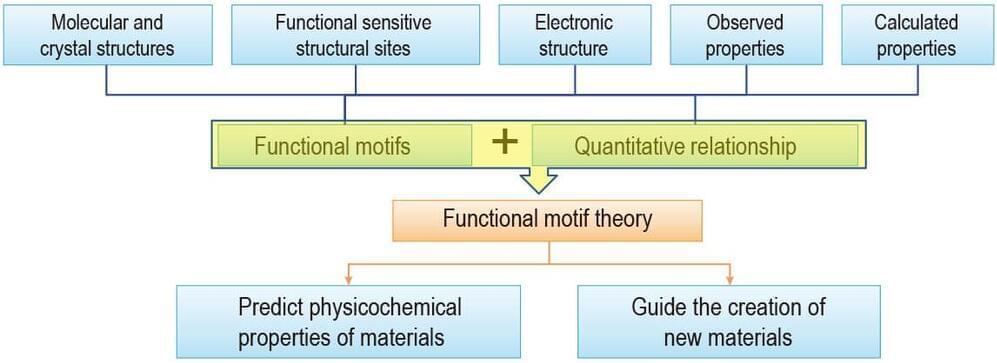
The traditional trial-and-error method in material research cannot meet the growing demand of various high performance materials, so developing a new effective paradigm of material science is extremely urgent. A study led by Dr. Xiao-Ming Jiang and Prof. Guo-Cong Guo (Fujian Institute of Research on the Structure of Matter, Chinese Academy of Sciences) proposes a new research paradigm for material studies based on the “functional motif” concept.
Functional motif was defined as the critical microstructure units (e.g., constituent components and building blocks) that play a decisive role in generating certain material functions. These units could not be replaced with other structure units without losing or significantly suppressing the relevant functions. The functional motif paradigm starts with the main aspects of microscopic structures and the properties of materials. On the basis of this understanding, the functional motifs governing the material properties can be extracted and the quantitative relationships between them can be investigated, and the results could be further developed as the “functional motif theory.” The latter should be useful as a guideline for creating new materials and as a tool for predicting the physicochemical properties of materials.
The properties of materials are determined by their functional motifs and how they are arranged in the materials, with the latter determining the quantitative structure–property relationships. Uncovering the functional motifs and their arrangements is crucial in understanding the properties of materials, and the functional motif exploration enables the rational design of new materials with desired properties.
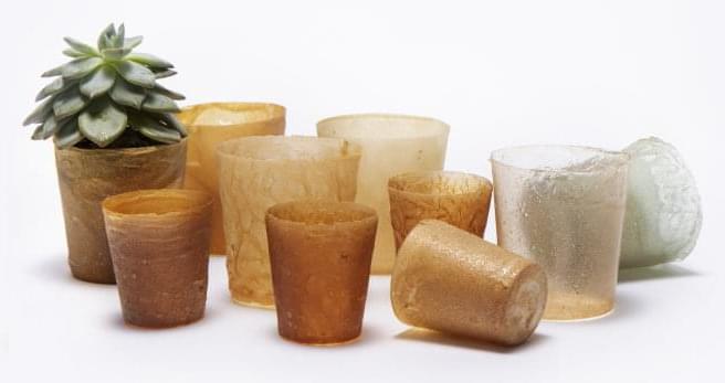
The four students are studying Innovation Design Engineering, a course delivered jointly by Imperial College London and the Royal College of Art. They have built a series of machines that extract, form and recycle the material, which they believe could be used as a replacement for various single-use plastics.
The project uses chitin, the world’s second most abundant biopolymer, (a naturally produced plastic). Chitin is found in crustaceans, insects and fungi, but needs to be chemically extracted from the source before it can be turned into the material.
The group of students have developed new manufacturing processes to transform lobster shell waste into biodegradable, recyclable bioplastic.
Adam FordAdmin.
I’m sure that’s not Deepmind’s official position atm — Nando de Freitas’s tweet was probably reactionary.
Nikolai Torp DragnesDoesn’t really read like the AGI is in a happy comfortable place does it? “Big red button,” “agents,” etc.? Sounds more like being locked in a cage with a gun to your head told to behave, told what to think, what to feel, what to do and what to look a… See more.
2 Replies.
View 11 more comments.
Shubham Ghosh Roy shared a link.
Every time a new cancer drug is announced, it represents hundreds of researchers spending years behind the scenes working to design and test a new molecule. The drug has to be not only effective, but also as safe as possible and easy to manufacture—and these researchers have to choose among thousands of possible options for its chemical structure.
But building each possible molecular structure for testing is a laborious process, even if researchers simply want to change a single carbon atom.
A new technique published by University of Chicago chemists and the pharmaceutical company Merck & Co. in the journal Science offers a way to leapfrog that process, allowing scientists to quickly and easily produce new molecules of interest.

A team of astronomers led by University of Michigan’s Ian Roederer and including Carnegie’s Erika Holmbeck have identified the widest range of elements yet observed in a star beyond our own Sun. Their findings will be published in The Astrophysical Journal Supplement Series.
The researchers identified 65 elements in the star, which is called HD 222925. Of these, 42 are from the bottom of the periodic table. Their identification will help astronomers better understand rapid neutron capture process — one of the main methods by which the universe’s heavy elements were created.
“To the best of my knowledge, that’s a record for any object beyond our Solar System. And what makes this star so unique is that it has a very high relative proportion of the elements listed along the bottom two-thirds of the periodic table. We even detected gold,” explained Roederer, a former Carnegie postdoc. “These elements were made by the rapid neutron capture process. That’s really the thing we’re trying to study: the physics in understanding how, where and when those elements were made.”
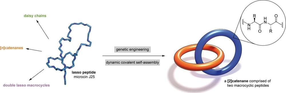
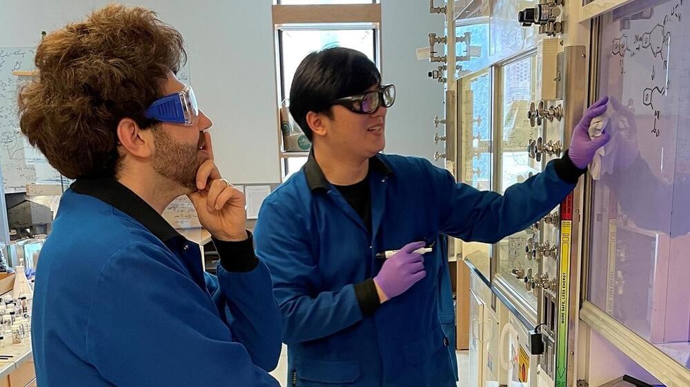
Researchers at Princeton University have built the world’s smallest mechanically interlocked biological structure, a deceptively simple two-ring chain made from tiny strands of amino acids called peptides.
In a paper published August 23 in Nature Chemistry, the team detailed a library of such structures made in their lab—two interlocked rings, a ring on a dumbbell, a daisy chain and an interlocked double lasso—each around one billionth of a meter in size. The study also demonstrates that some of these structures can toggle between at least two shapes, laying the groundwork for a biomolecular switch.
“We’ve been able to build a bunch of structures that no one’s been able to build before,” said A. James Link, professor of chemical and biological engineering, the study’s principal investigator. “These are the smallest threaded or interlocking structures you can make out of peptides.”
The chemical composition and presence of metallic fragments also make lunar soil-less suitable for plant growth as compared to volcanic ash. However, the biggest takeaway from this experiment is still that scientists have somehow grown a plant in a soil sample taken from the Moon.
Emphasizing the importance of this result co-author and geologist Stephen Elardo said, from a geology standpoint, I look at this soil as being very very different from any soil you will find here on Earth. I think it’s amazing the plant still grows, right. It’s stressed, but it doesn’t die. It doesn’t fail to grow at all, it adapts.
The researchers also highlight that further research can enable us to know the ways plants can be efficiently grown on the Moon. Therefore, through related studies, we need to better understand how Earth plants interact with lunar soil.