Toggle light / dark theme

Did product safety laws lead to the dumbing down of science toys?


“Users should not take ore samples out of their jars, for they tend to flake and crumble and you would run the risk of having radioactive ore spread out in your laboratory.” Such was the warning that came with the Gilbert U-238 Atomic Energy Lab, a 1950s science kit that included four small jars of actual uranium. Budding young nuclear scientists were encouraged to use the enclosed instruments to measure the samples’ radioactivity, observe radioactive decay, and even go prospecting for radioactive ores. Yes, the Gilbert company definitely intended for kids to try this at home. And so the company’s warning was couched not in terms of health risk but rather as bad scientific practice: Removing the ore from its jar would raise the background radiation, thereby invalidating your experimental results.

The Gilbert U-238 Atomic Energy Lab put a positive spin on radioactivity

Along with personal jetpacks for every man, woman, and child (sure, why not), levitation is one of those conveniences that sci-fi has long promised us but has yet to deliver, other than magnetically levitating trains. But at Argonne National Laboratory in Illinois, physicist Chris Benmore and his colleagues are levitating objects with an unlikely tool: sound. It’s called acoustic levitation, and after breaking your brain with what seems to be an optical illusion, it’s poised to deliver advances in pharmacology, chemistry more broadly, and even robotics.

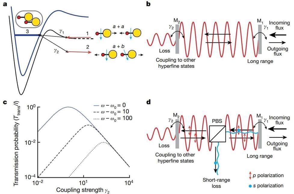
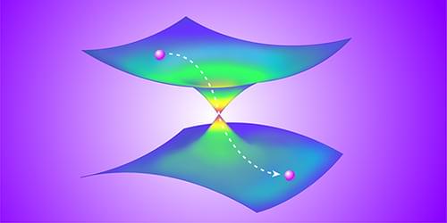
The concept of universal physics is intriguing, as it enables researchers to relate physical phenomena in a variety of systems, irrespective of their varying characteristics and complexities. Ultracold atomic systems are often perceived as ideal platforms for exploring universal physics, owing to the precise control of experimental parameters (such as the interaction strength, temperature, density, quantum states, dimensionality, and the trapping potential) that might be harder to tune in more conventional systems. In fact, ultracold atomic systems have been used to better understand a myriad of complex physical behavior, including those topics in cosmology, particle, nuclear, molecular physics, and most notably, in condensed matter physics, where the complexities of many-body quantum phenomena are more difficult to investigate using more traditional approaches.

Understanding the applicability and the robustness of universal is thus of great interest. Researchers at the National Institute of Standards and Technology (NIST) and the University of Colorado Boulder have carried out a study, recently featured in Physical Review Letters, aimed at testing the limits to universality in an ultracold system.

“Unlike in other physical systems, the beauty of ultracold systems is that at times we are able to scrap the importance of the periodic table and demonstrate the similar phenomenon with any chosen atomic species (be it potassium, rubidium, lithium, strontium, etc.),” Roman Chapurin, one of the researchers who carried out the study, told Phys.org. “Universal behavior is independent of the microscopic details. Understanding the limitations of universal phenomenon is of great interest.”

A, C57BL/6J mice were genetically engineered using CRISPR–Cas9 genomic editing to encode 288L and 330R in mDPP4 on one chromosome (heterozygous, 288/330+/−) or on both chromosomes (homozygous, 288/330+/+). b, Northern blot of mDPP4 mRNA expression. c, Immunohistochemistry (IHC) of mDPP4 protein in the lungs, brain and kidneys of individual C57BL/6J wild-type (WT), 288/330+/− and 288/330+/+ mice. d, Viral titres for MERS-CoV at 3 days post-infection from C57BL/6J WT, 288/330+/− and 288/330+/+ (all n = 4) mice infected with 5 × 10⁵ plaque-forming units (p.f.u.) of the indicated viruses. Bar graphs show means + s.d.

In a new report published on Scientific Reports, Milan M. Milošević and an international research team at the Zepler Institute for Photonics and Nanoelectronics, Etaphase Incorporated and the Departments of Chemistry, Physics and Astronomy, in the U.S. and the U.K. Introduced a hyperuniform-disordered platform to realize near-infrared (NIR) photonic devices to create, detect and manipulate light. They built the device on a silicon-on-insulator (SOI) platform to demonstrate the functionality of the structures in a flexible, silicon-integrated circuit unconstrained by crystalline symmetries. The scientists reported results for passive device elements, including waveguides and resonators seamlessly integrated with conventional silicon-on-insulator strip waveguides and vertical couplers. The hyperuniform-disordered platform improved compactness and enhanced energy efficiency as well as temperature stability, compared to silicon photonic devices fabricated on rib and strip waveguides.

Academic and commercial efforts worldwide in the field of silicon photonics have led to engineer optical data communications at the Terabit-scale at increasingly lower costs to meet the rapidly growing demand in data centers. Explosive growth in cloud computing and entertainment-on-demand pose increasingly challenging costs and energy requirements for , processing and storage. Optical interconnects can replace traditional copper-based solutions to offer steadily increasing potential to minimize latency and , while maximizing the bandwidth and reliability of the devices. Silicon photonics also leverage large-scale, complementary metal-oxide semiconductor (CMOS) manufacturing processes to produce high-performance optical transceivers with high yield at low-cost. The properties allow applications of optical transceivers (fiber optical technology to send and receive data) to be increasingly compelling across shorter distances.

More than three decades ago, physicist Richard Soref identified silicon as a promising material for photonic integration. Leading to the present-day steady development and rapid production of increasingly complex photonic integrated circuits (PICs). Researchers can integrate large numbers of massively-parallel compact energy-efficient optical components on a single chip for cloud computing applications from deep learning to artificial intelligence and the internet of things. Compared to the limited scope of commercial silicon photonic systems, photonic crystal (PhC) architectures promise smaller device sizes, although they are withheld by layout constraints imposed by waveguide requirements along the photonic crystal’s axis. Until recently, photonic band gap (PBG) structures that efficiently guide light were limited to photonic crystal platforms. Now, newer classes of PBG structures include photonic quasicrystals, hyperuniform disordered solids (HUDs) and local self-uniform structures.

The accelerator-on-a-chip demonstrated in Science is just a prototype, but Vuckovic said its design and fabrication techniques can be scaled up to deliver particle beams accelerated enough to perform cutting-edge experiments in chemistry, materials science and biological discovery that don’t require the power of a massive accelerator.

“The largest accelerators are like powerful telescopes. There are only a few in the world and scientists must come to places like SLAC to use them,” Vuckovic said. “We want to miniaturize accelerator technology in a way that makes it a more accessible research tool.”

Team members liken their approach to the way that computing evolved from the mainframe to the smaller but still useful PC. Accelerator-on-a-chip technology could also lead to new cancer radiation therapies, said physicist Robert Byer, a co-author of the Science paper. Again, it’s a matter of size.

Today, medical X-ray machines fill a room and deliver a beam of radiation that’s tough to focus on tumors, requiring patients to wear lead shields to minimize collateral damage.