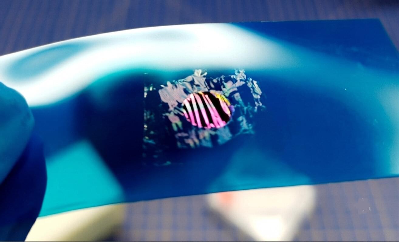
Scientists have unveiled a new fabrication technique for the ultra-clean manufacturing of 2D heterostructures—materials just a few atoms thick—that could be used in quantum technology and electronics. Experts from Southampton and Singapore say the method could be used to develop next-generation devices that accelerate research in quantum computing.
The research behind their technique, published in Nature Communications, was developed in collaboration between the Institute for Functional Intelligent Materials at the National University of Singapore and the University of Southampton.
Current manufacturing methods to build two-dimensional materials rely on sticky synthetic polymers to assemble the atomic layers. However, these often leave behind microscopic residues that contaminate the tiny structures and disrupt the performance of electronic devices that use them. The research team instead used the natural mineral muscovite, or mica, to stack the atomically thin materials together.