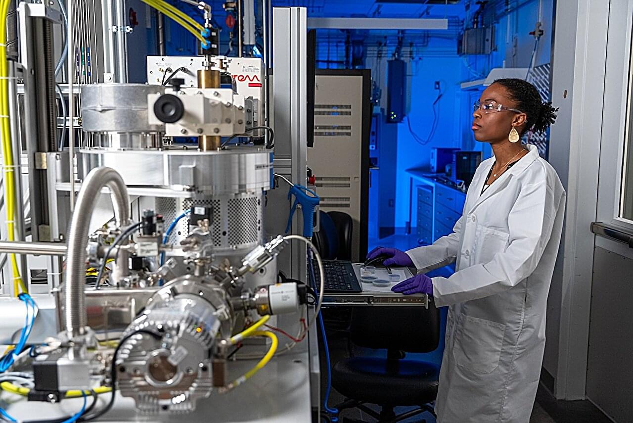
Materials scientists at Rice University have developed a new workflow methodology for measuring microscopic defects in diamond and other advanced semiconductor materials. By making it easier to spot flaws that can undermine performance, the approach could accelerate the development of more reliable electronic and quantum devices.
The research team developed a custom Python-based software tool to rapidly analyze data from high-resolution X-ray diffraction, a technique that uses X-rays to probe a material’s internal crystal structure. The software analyzes the resulting diffraction patterns, picks up on dislocations and irregularities in the atomic lattice, and calculates their density in a given material.
“Dislocations can disrupt how charge and heat move through the material, which impacts how efficient and reliable a device is and how easy it is to manufacture at scale,” said Xiang Zhang, assistant research professor of materials science and nanoengineering at Rice and a corresponding author on the study published in Advanced Materials.