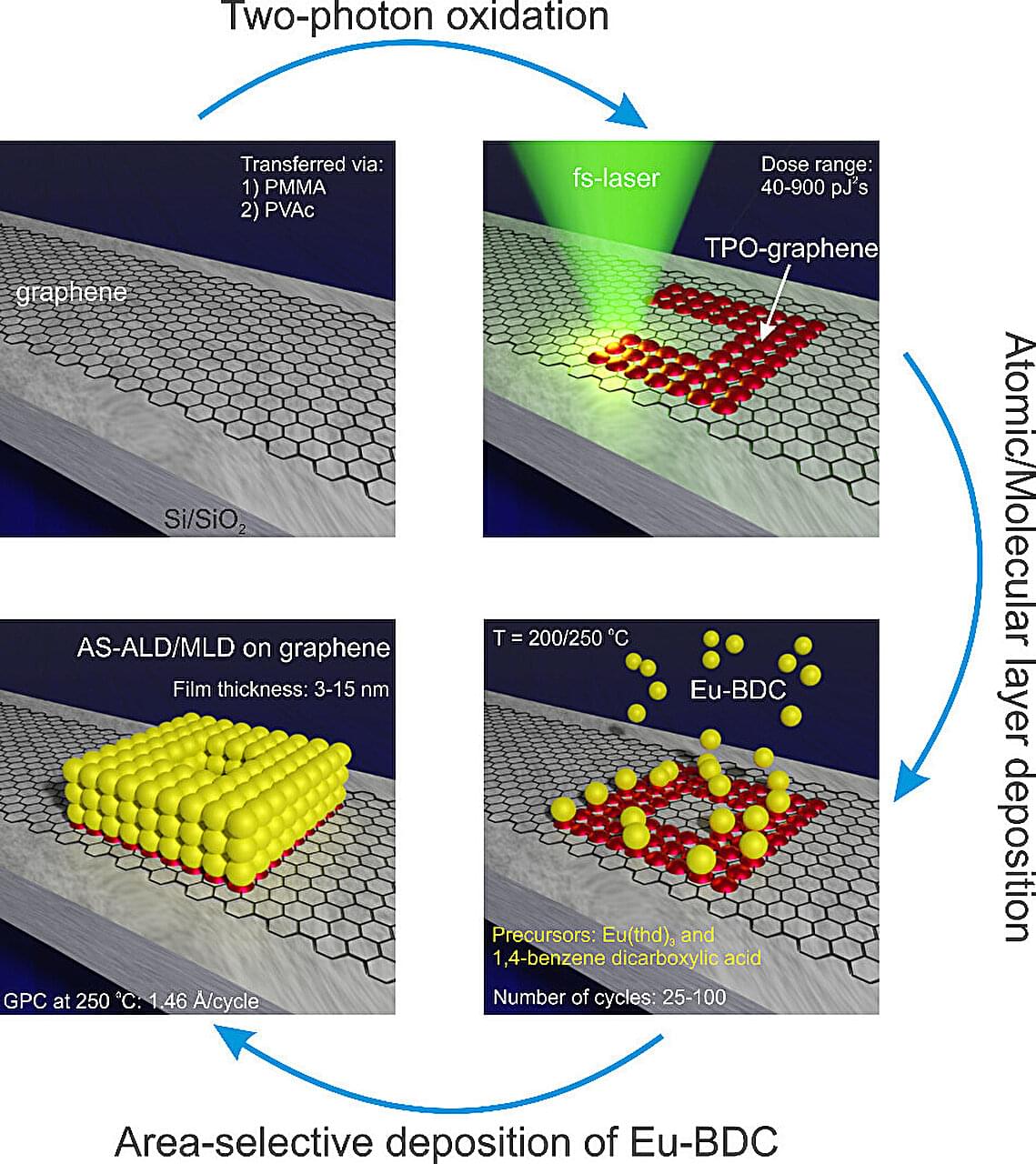
Researchers from the University of Jyväskylä and Aalto University have developed a new method based on laser modification, which allows metal-organic materials to be grown locally one molecule-thick layer at a time. The method enables the precise construction of films of different shapes and offers new ways to modify the properties of materials for various applications. The study was published in the journal ACS Nano.
Atomic layer deposition (ALD) is a method used especially in the semiconductor industry to produce high-quality thin films with atomic layer accuracy. The method was developed in the 1970s by the Finnish Tuomo Suntola, and it has since become an important technology.
In ALD, thin films are grown one atomic layer at a time through controlled chemical reactions between the reactants, as well as their interactions with the surface. This so-called bottom-up method allows for precise film thickness adjustment.