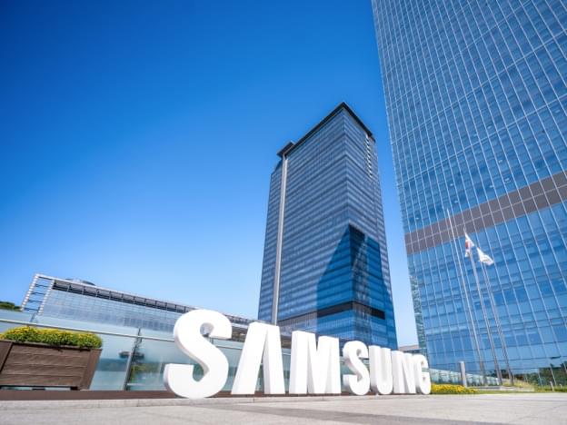
With AI compute demands soaring, silicon photonics is emerging as a next-generation technology poised to reshape the landscape. According to Hankyung, sources say that Samsung Electronics’ Device Solutions (DS) Division has designated the technology as a future strategic priority and begun recruiting experts for its Singapore-based R&D center, led by Vice President King-Jien Chui, a former TSMC executive. The report highlights that Samsung is expanding its team in Singapore and working with Broadcom to move the technology toward commercialization.
As the report indicates, citing industry sources, Samsung’s 2027 target for CPO (Co-Packaged Optics) commercialization suggests that its real contest with TSMC will begin at that point. By 2030—when silicon photonics is expected to be applied at the individual-chip level—the technology will likely become the central battleground of the foundry market. Although TSMC currently leads, Samsung is gearing up, viewing the technology as a key to attracting major foundry clients, the report adds.
