A team led by researchers at Rensselaer Polytechnic Institute (RPI) has made a breakthrough in semiconductor development that could reshape the way we produce computer chips, optoelectronics and quantum computing devices.
The team, which also includes researchers from the National High Magnetic Field Laboratory, Florida State University and SUNY Buffalo, published their findings last month in Nature. Their work deepens the understanding of remote epitaxy, a manufacturing technique that entails growing high-quality semiconducting films on one substrate and then transferring them to a different one.
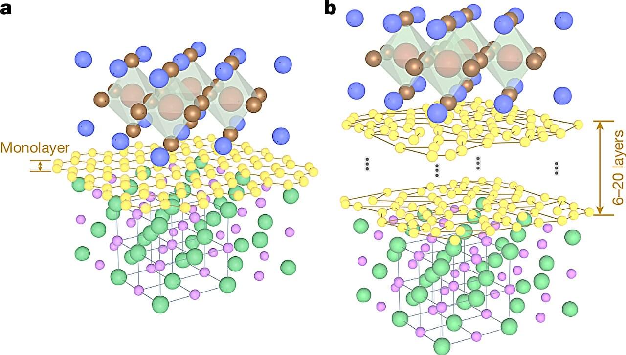
Remote epitaxy works by placing a thin buffer layer between a substrate and a growing crystal film. The substrate’s atomic structure guides the crystal’s growth through the buffer, but the buffer prevents permanent bonding—meaning that the finished crystal layer can be peeled off and moved elsewhere.