Researchers at the National University of Singapore (NUS) have observed a doping-tunable charge density wave (CDW) in a single-layer semiconductor, Chromium(III) selenide (Cr2Se3), extending the CDW phenomenon from metals to doped semiconductors.
CDWs are intriguing electronic patterns widely observed in metallic two-dimensional (2D) transition metal chalcogenides (TMCs). The study of CDW provides insights into emergent orders in quantum materials, where electron correlations play a non-negligible role. However, most reported TMCs exhibiting CDW are intrinsic metals, and tuning their carrier density is predominantly accomplished through intercalation or atomic substitution. These approaches may introduce impurities or defects that complicate the understanding of the underlying mechanisms.
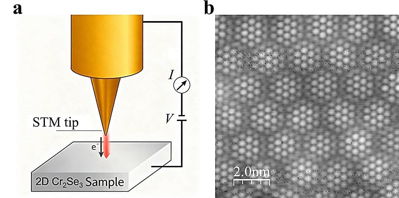
A research team led by Professor Chen Wei from the Department of Physics and the Department of Chemistry at NUS, synthesized single-layer semiconducting Cr2Se3 and demonstrated the CDW phenomenon using scanning tunneling microscopy (STM).