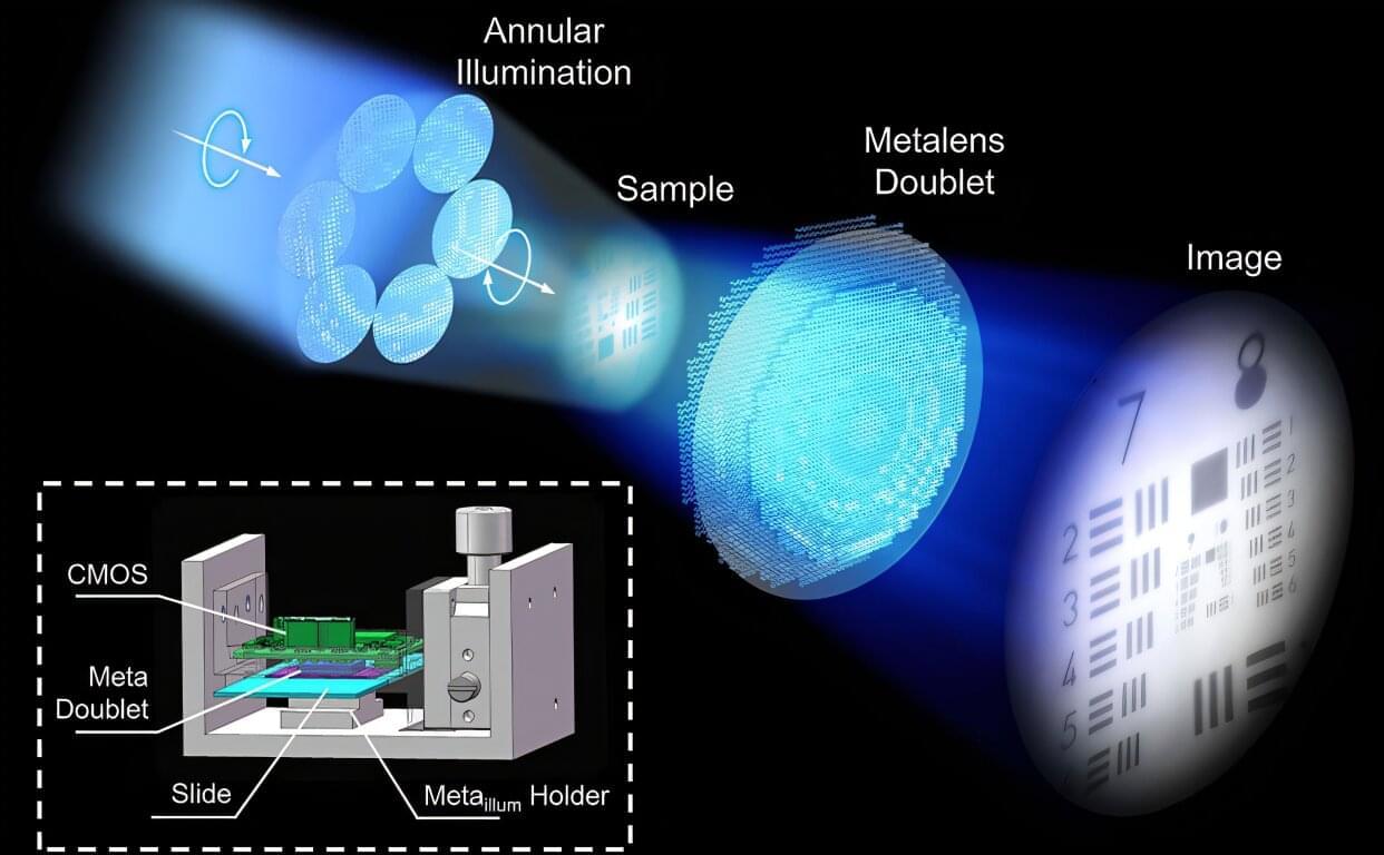
Metalenses represent a revolutionary advancement in optical technology. Unlike conventional microscope objectives that rely on curved glass surfaces, metalenses employ nanoscale structures to manipulate light at the subwavelength level. Thanks to their ultrathin, lightweight, and flat architectures, metalenses can overcome the bulkiness of traditional lenses, making them ideal candidates for integration in electronic devices and compact imaging systems.
Despite their promising attributes for next-generation optical systems, metalenses face significant challenges in practical microscopy applications. Off-axis aberrations, which severely restrict metalens field of view (FOV) and resolution capabilities, are primary limitations.
The inherent trade-off between imaging resolution and FOV has prevented metalenses from achieving performance comparable to conventional microscopes. Although some prior metalens designs have achieved submicron resolution, they operated with an extremely restricted FOV, limiting their practical utility.