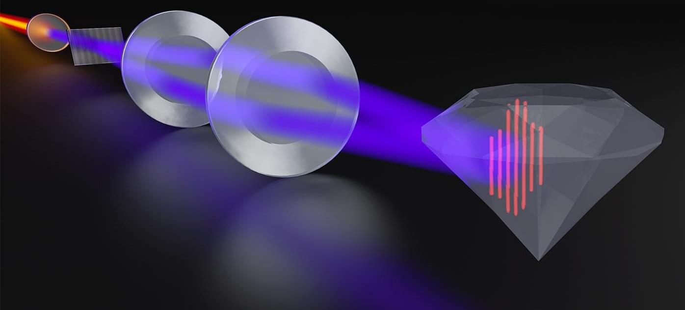
Ultrawide-bandgap semiconductors—such as diamond—are promising for next-generation electronics due to a larger energy gap between the valence and conduction bands, allowing them to handle higher voltages, operate at higher frequencies, and provide greater efficiency compared to traditional materials like silicon.
However, their unique properties make it challenging to probe and understand how charge and heat move on nanometer-to-micron scales. Visible light has a very limited ability to probe nanoscale properties, and moreover, it is not absorbed by diamond, so it cannot be used to launch currents or rapid heating.
Now, researchers at JILA, led by JILA Fellows and University of Colorado physics professors Margaret Murnane and Henry Kapteyn, along with graduate students Emma Nelson, Theodore Culman, Brendan McBennett, and former JILA postdoctoral researchers Albert Beardo and Joshua Knobloch, have developed a novel microscope that makes examining these materials possible on an unprecedented scale.
