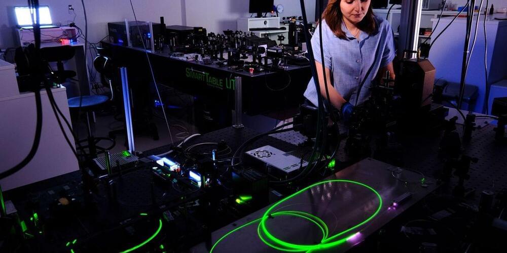
Modern computer chips can have features built on a nanometer scale. Until now it has been possible to form such small structures only on top of a silicon wafer, but a new technique can now create nanoscale features in a layer below the surface. The approach has promising applications in both photonics and electronics, say its inventors, and could one day enable the fabrication of 3D structures throughout the bulk of the wafer.
The technique relies on the fact that silicon is transparent to certain wavelengths of light. This means the right kind of laser can travel through the surface of the wafer and interact with the silicon below. But designing a laser that can pass through the surface without causing damage and still carry out precise nanoscale fabrication below is not simple.
Researchers from Bilkent University in Ankara, Türkiye, achieved this by using spatial light modulation to create a needlelike laser beam that gave them greater control over where the beam’s energy was deposited. By exploiting physical interactions between the laser light and the silicon, they were able to fabricate lines and planes with different optical properties that could be combined to create nanophotonic elements below the surface.
