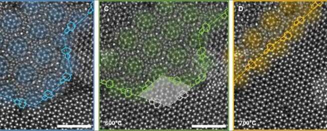
Silicon-based electronics are approaching their physical limitations and new materials are needed to keep up with current technological demands. Two-dimensional (2D) materials have a rich array of properties, including superconductivity and magnetism, and are promising candidates for use in electronic systems, such as transistors. However, precisely controlling the properties of these materials is extraordinarily difficult.
