The dynamic characteristics of the inverters have been simulated by varying the inverter output (load) capacitance (COUT), connected to the inverter output across a 1000 nm long interconnect (assumed for simulations of the NM circuit, described in “NM circuit” subsection), from 1 aF to 1 fF. By evaluating the delay \(({t}_{{{{{{\rm{p}}}}}}})\) of the input-to-outpution, and the instantaneous current drawn from the supply during thision, the average power dissipation, and the energy-delay-product (EDP), is evaluated for both the 2D-TFET and the FinFET implementations. The higher delay of the 2D-TFET (due to its lower ON-current) translates to higher EDP, and the EDP metrics get worse as the load capacitance is further increased. In fact, as will be shown later, the main advantages of TFETs are in implementations of sparse switching circuits where its much lower OFF-current and small SS help in lowering the static power dissipation, thereby improving the overall performance.
Figure 2c shows an 11-stage ring oscillator, implemented considering both interconnect and device parasitics, and designed with minimum sized 2D-TFET and FinFET inverters. Figure 2 d, e compares the transient characteristics of the FinFET and the 2D-TFET ring oscillators, from which the frequency of oscillation is extracted to be 10 GHz and 57 MHz, respectively, corresponding to single-stage delays of 10 ps and 1.6 ns. The delay of the 2D-TFET ring oscillator is larger due to its lower ON-current. The effect of the enhanced Miller capacitance in creating large overshoots and undershoots of the output voltage in TFETs is also observed in Fig. 2e.
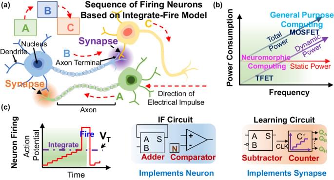
Static random-access memory (SRAMs), which occupy up to 70% of the processor area are the main memory elements in designing CPU cache memory offering fast memory access and can be used for synapse weight retention in a designed NM system comprising of several neurons. However, this large prevalence of SRAMs also results in a large power consumption. In fact, SRAM data access in Intel’s Loihi5 has been estimated to be more energy intensive than each neuronal spike, necessitating the development of low-power SRAM implementations. Although SRAM design with 2D-TFETs can improve the energy-efficiency, the standard SRAM design utilizes two access transistors for operation, which require bidirectional current flow, and are therefore, ill-suited for implementation with unidirectional-TFETs. This necessitates the development of a modified SRAM design, which either uses a pass transistor network of TFETs, or solitary 2D-FETs, for implementing the function of the access transistors (Fig. 2f–l).