Ben Dixon, a researcher in the Optical and Quantum Communications Technology Group, explains how the process works: “First, you need to generate pairs of specific entangled qubits (called Bell states) and transmit them in different directions across the network link to two separate quantum repeaters, which capture and store these qubits. One of the quantum repeaters then does a two-qubit measurement between the transmitted and stored qubit and an arbitrary qubit that we want to send across the link in order to interconnect the remote quantum systems. The measurement results are communicated to the quantum repeater at the other end of the link; the repeater uses these results to turn the stored Bell state qubit into the arbitrary qubit. Lastly, the repeater can send the arbitrary qubit into the quantum system, thereby linking the two remote quantum systems.”
To retain the entangled states, the quantum repeater needs a way to store them — in essence, a memory. In 2020, collaborators at Harvard University demonstrated holding a qubit in a single silicon atom (trapped between two empty spaces left behind by removing two carbon atoms) in diamond. This silicon “vacancy” center in diamond is an attractive quantum memory option. Like other individual electrons, the outermost (valence) electron on the silicon atom can point either up or down, similar to a bar magnet with north and south poles. The direction that the electron points is known as its spin, and the two possible spin states, spin up or spin down, are akin to the ones and zeros used by computers to represent, process, and store information. Moreover, silicon’s valence electron can be manipulated with visible light to transfer and store a photonic qubit in the electron spin state. The Harvard researchers did exactly this; they patterned an optical waveguide (a structure that guides light in a desired direction) surrounded by a nanophotonic optical cavity to have a photon strongly interact with the silicon atom and impart its quantum state onto that atom. Collaborators at MIT then showed this basic functionality could work with multiple waveguides; they patterned eight waveguides and successfully generated silicon vacancies inside them all.
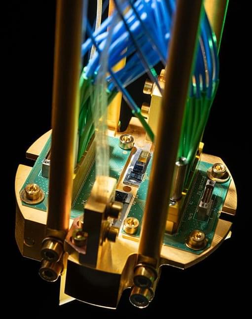
Lincoln Laboratory has since been applying quantum engineering to create a quantum memory module equipped with additional capabilities to operate as a quantum repeater. This engineering effort includes on-site custom diamond growth (with the Quantum Information and Integrated Nanosystems Group); the development of a scalable silicon-nanophotonics interposer (a chip that merges photonic and electronic functionalities) to control the silicon-vacancy qubit; and integration and packaging of the components into a system that can be cooled to the cryogenic temperatures needed for long-term memory storage. The current system has two memory modules, each capable of holding eight optical qubits.