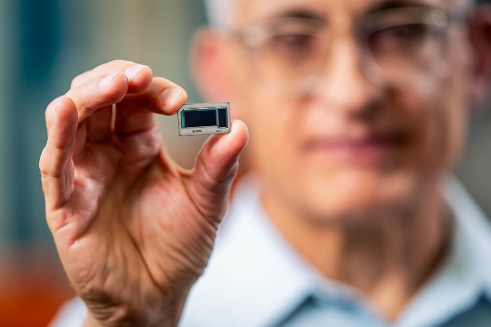
While semiconductor lithography gets the bulk of the attention in chipmaking, other processes are equally important in producing working integrated circuits (ICs). Case in point: packaging. An IC package provides the electrical, thermal, and mechanical transition from the semiconductor die or chip to the circuit board, which is often called a motherboard. One key element of the IC package is the substrate, which is essentially a miniature circuit board with copper traces that bonds to the input/output (I/O), power and ground pads on the chip and electrically connects these pads to the circuit board. The substrate provides a solid mechanical home for the chip and is also thermally matched to… More.
The release also quotes Babak Sabi, Intel senior vice president and general manager of Assembly and Test Development, who said: “After a decade of research, Intel has achieved industry-leading glass substrates for advanced packaging. We look forward to delivering these cutting-edge technologies that will benefit our key players and foundry customers for decades to come.”
Research into using glass substrates for chipmaking is nothing new. As Intel’s release says, the company has been working on this technology for at least a decade, as have other organizations such as the 3D Systems Packaging Research Center located at Georgia Tech, which was founded in 1994 – nearly 30 years ago. Last year, the Georgia Tech PRC launched an industry advisory board with Intel Fellow Ravi Mahajan as one of the initial board members. Intel has already spent more than a billion dollars to develop a glass-substrate manufacturing facility at its site in Chandler, Arizona.
So, if glass IC substrates are nothing new, why would Intel announce this particular development now, after ten years of corporate development and several years before these substrates find their way into products? On the technical side, it’s because existing ceramic and organic substrates are reaching the end of their ability to provide the electrical, thermal, and mechanical transitions for today’s most advanced semiconductors, which is doubly true as the industry adopts chiplets as an increasingly common way to put more transistors into a package.