Carbon nanotubes, large cylindrical molecules composed of hybridized carbon atoms arranged in a hexagonal structure, recently attracted significant attention among electronics engineers. Due to their geometric configuration and advantageous electronic properties, these unique molecules could be used to create smaller field-effect transistors (FETs) that exhibit high energy efficiencies.
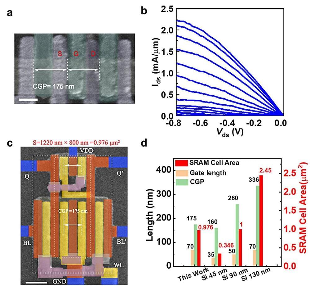
FETs based on carbon nanotubes have the potential to outperform smaller transistors based on silicon, yet their advantage in real-world implementations has yet to be conclusively demonstrated. A recent paper by researchers at Peking University and other institutes in China, published in Nature Electronics, outlines the realization of FETs based on carbon nanotubes that can be scaled to the same size of a 10 nm silicon technology node.
“Recent progress in achieving wafer-scale high density semiconducting carbon nanotube arrays brough us one step closer to the practical use of carbon nanotubes in CMOS circuits,” Zhiyong Zhang, one of the researchers who carried out the study, told Phys.org. “However, previous research efforts have mainly focused on the scaling of channel or gate length of carbon nanotube transistors while keeping large contact dimensions, which cannot be accepted for high density CMOS circuits in practical applications.