Since the first High-Bandwidth Memory (HBM) stacks were introduced in 2013, these stacked memory chiplets have carved out a new, high-performance niche for DRAM in the memory hierarchy. The first products to incorporate HBM started to appear in 2015. You will now find HBM stacks in high-end CPUs, GPUs, and FPGAs, where performance matters more than cost to the end customer. Although HBM is not as fast as SRAM, it is faster than bulk DDR memory, and it’s getting even faster. Micron has just announced what the company is calling a “second-generation” (Gen 2) HBM3 DRAM that adheres to the semiconductor industry’s “bigger, better, faster” mantra. Because it integrates higher-density DRAM die, Micron’s HBM3 Gen 2 can be 50 percent bigger (higher capacity) than existing HBM3 DRAM available from other memory vendors, with 2.5x better performance/power ratings and 50 percent faster speed (1.2Tbytes/second). That’s the DRAM industry’s equivalent of a trifecta.
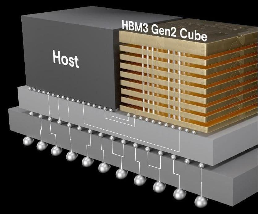
HBM is akin to a chiplet skyscraper. Each HBM stack consists of a logic die, which contains a system interface and DRAM control, with multiple DRAM die stacked on top of the logic die. The entire stack is designed to be incorporated into an IC package along with larger semiconductor die and other, smaller chiplets. You’ll find earlier HBM generations incorporated into server CPUs from AMD and Intel, FPGAs from AMD and Intel, and GPUs from AMD, Intel, and Nvidia. The most recent announcement of a GPU containing HBM is AMD’s MI300X GPU, announced by the company’s CEO Lisa Su in June. (See “AMD Hops On The Generative AI Bandwagon With Instinct MI300X.”) Intel previously announced HBM use in the company’s Data Center GPU Max Series, the data center GPU formerly known as Ponte Vecchio. Nvidia’s H100 Hopper GPU also incorporates HBM memory stacks.
Micron has now entered the HBM3 race with what the company is calling a “second-generation” HBM3 design, because Micron’s version of an HBM3 stack is arriving about a year after competitive products, but is based on a faster, denser, more advanced semiconductor process node. The DRAM die in this Micron HBM3 stack is being fabricated with the company’s 1β process technology, which the company announced last year. During that announcement, the company claimed that the 1β process increased DRAM bit density by 35 percent and decreased power consumption by 15 percent, when compared to the company’s 1α node. At the time, Micron announced plans to use its 1β process node for manufacturing DDR5 and LPDDR5 DRAM. The company has now stated that they will use the same process node for manufacturing DRAM die for its HBM3 stacks.