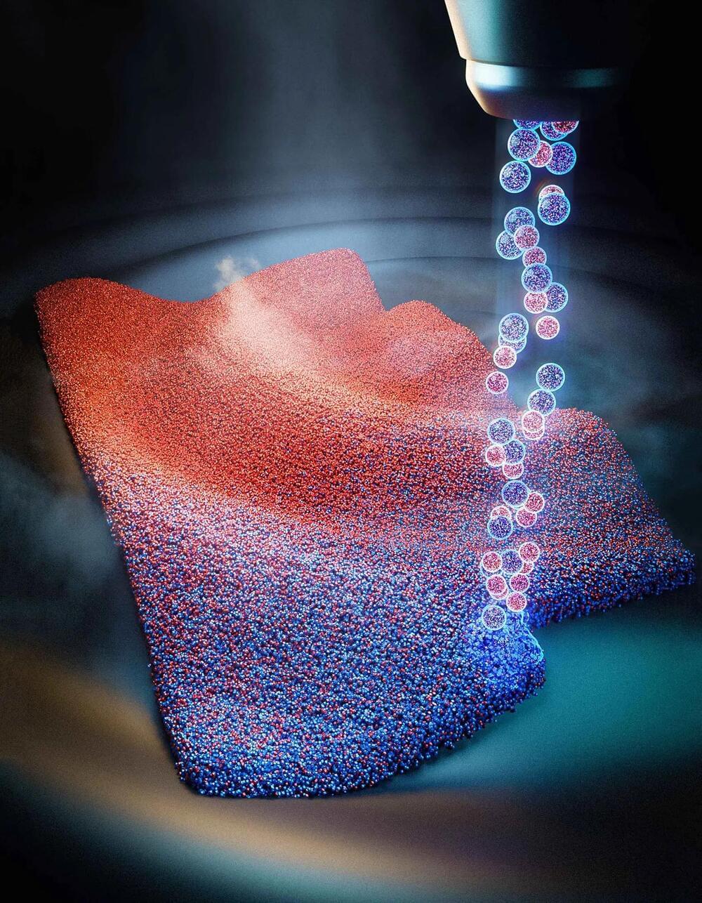
A novel 3D printing method called high-throughput combinatorial printing (HTCP) has been created that significantly accelerates the discovery and production of new materials.
The process involves mixing multiple aerosolized nanomaterial inks during printing, which allows for fine control over the printed materials’ architecture and local compositions. This method produces materials with gradient compositions and properties and can be applied to a wide range of substances including metals, semiconductors.
Semiconductors are a type of material that has electrical conductivity between that of a conductor (such as copper) and an insulator (such as rubber). Semiconductors are used in a wide range of electronic devices, including transistors, diodes, solar cells, and integrated circuits. The electrical conductivity of a semiconductor can be controlled by adding impurities to the material through a process called doping. Silicon is the most widely used material for semiconductor devices, but other materials such as gallium arsenide and indium phosphide are also used in certain applications.
