Discovered in 2004, graphene has revolutionized various scientific fields. It possesses remarkable properties like high electron mobility, mechanical strength, and thermal conductivity. Extensive time and effort has been invested in exploring its potential as a next-generation semiconductor material, leading to the development of graphene-based transistors, transparent electrodes, and sensors.
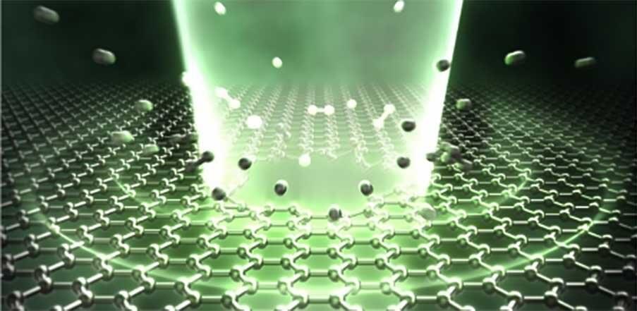
But to render these devices into practical application, it’s crucial to have efficient processing techniques that can structure graphene films at micrometer and nanometer scale. Typically, micro/nanoscale material processing and device manufacturing employ nanolithography and focused ion beam methods. However, these have posed longstanding challenges for laboratory researchers due to their need for large-scale equipment, lengthy manufacturing times, and complex operations.
In January 2023, Tohoku University researchers created a technique that could micro/nanofabricate silicon nitride devices with thicknesses ranging from five to 50 nanometers. The method employed a femtosecond laser, which emitted extremely short, rapid pulses of light. It turned out to be capable of quickly and conveniently processing thin materials without a vacuum environment.