Circa 2016 face_with_colon_three
A transistor laser (TL)1,2,3, having the structure of a transistor with multi-quantum wells (MQWs) near its base region, bridges the functionality gap between lasers and transistors. From a TL, an electrical signal can be outputted simultaneously with a light signal by inputting one electrical signal, making it suitable for future high performance optoelectronic integrated device applications4. As a new kind of semiconductor laser or transistor, TLs have aroused many interests since its invention. For example, in 2006, the paper2 reporting the first room temperature operation of TLs was voted as one of the five most important papers published by Applied Physics Letters in over 40 years5. Because of the transistor structure, many interesting characters have been demonstrated, including resonance free frequency response, large direct modulation band width6, voltage controlled mode of operation7, low relative intensity noise (RIN) close to the shot-noise limit8 and low 3rd order intermodulation distortion (IMD)9.
However, light emission for all the TLs reported up to now is produced at the expense of current gain. Taking npn TLs as an example, in the devices, electrons injected from the emitter into the base layer first recombine with holes radiatively before the left being collected by the collector4. The majority of the electrons are consumed by stimulated light emissions, leading to a current gain which is a lot lower than the gain of a traditional transistor. The common emitter (CE) mode current gain (collector current/base current) is lower than 5 for most, if not all, of the TLs studied, either experimentally1,2,3,6,7,8,9,10 or numerically11,12,13. The low current gain may limit the performance of systems that use TLs. For example, it is much easier to integrate monolithically a heterojunction bipolar transistor (HBT) and a TL than to integrate an HBT with a laser diode (LD) because of the dual functionality of TLs. For such applications, a large current gain of TL (used as HBT) is desired for the amplification of electrical signal to drive the laser.
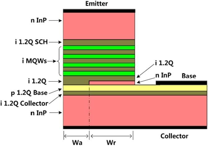
In this work, we propose a novel TL structure which has an n-doped InP layer inserted in the emitter ridge, forming a flow aperture in the center of the emitter ridge for only holes. Here after, the TLs having the hole current aperture is designated as a-TLs. The properties of the a-TLs are systematically studied numerically. It is shown that while the light emission power of a-TLs is comparable with that of TLs without the aperture at the same base current, the CE current gain of a-TLs can be over 15 times larger.