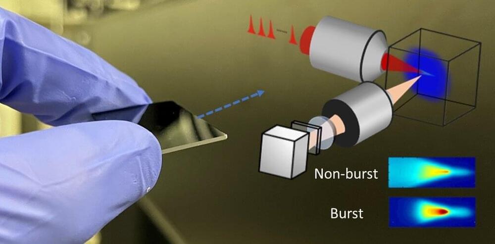
Researchers from LP3 Laboratory in France developed a light-based technique for local material processing anywhere in the three-dimensional space of semiconductor chips. The direct laser writing of new functionalities opens the possibility to exploit the sub-surface space for higher integration densities and extra functions.
Semiconductors remain the backbone material of the electronics integrated with modern devices such as cellphones, cars, robots and many other intelligent devices. Driven by the continuous need for miniaturized and powerful chips, the current semiconductor manufacturing technologies are facing increasing pressure.
The dominating manufacturing technology, lithography, has strong limitations when addressing these challenges, given its surface processing nature. For this reason, a solution to fabricating structures under the wafer surfaces would be highly desirable so that the full space inside the materials could be exploited.