It’s a problem that few of us will likely ever face: once you’ve built your first homemade integrated circuit, what do you do next? If you’re [Sam Zeloof], the answer is clear: build better integrated circuits.
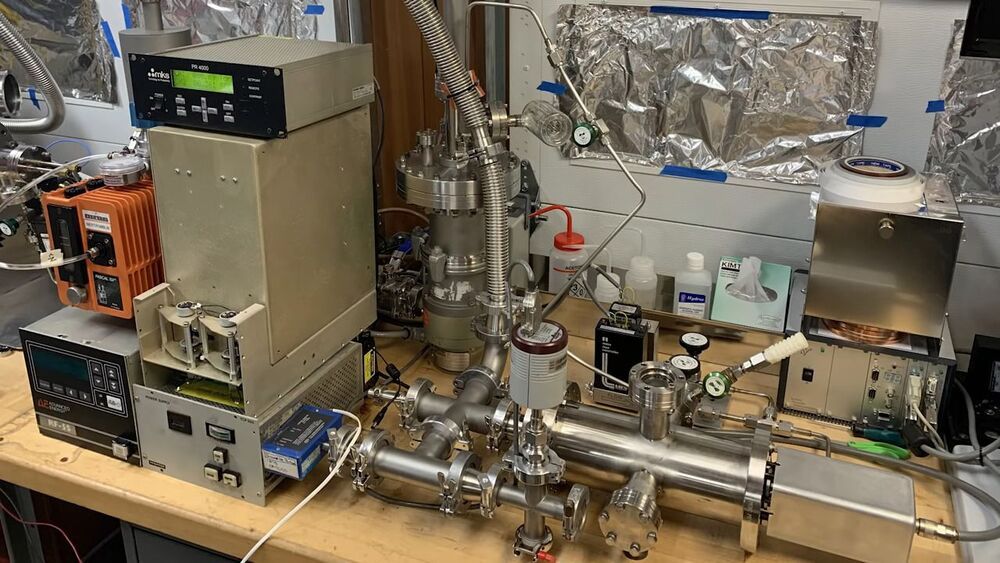
At least that’s [Sam]’s plan, which his new reactive-ion etching setup aims to make possible. While his Z1 dual differential amplifier chip was a huge success, the photolithography process he used to create the chip had its limitations. The chemical etching process he used is a bit fussy, and prone to undercutting of the mask if the etchant seeps underneath it. As its name implies, RIE uses a plasma of highly reactive ions to do the etching instead, resulting in finer details and opening the door to using more advanced materials.
[Sam]’s RIE rig looks like a plumber’s stainless steel nightmare, in the middle of which sits a vacuum chamber for the wafer to be etched. After evacuating the air, a small amount of fluorinated gas — either carbon tetrafluoride or the always entertaining sulfur hexafluoride — is added to the chamber. A high-voltage feedthrough provides the RF energy needed to create a plasma, which knocks fluorine ions out of the process gas. The negatively charged and extremely reactive fluorine ions are attracted to the wafer, where they attack and etch away the surfaces that aren’t protected by a photoresist layer.