Advanced system-on-chip designs are extremely complex in terms of transistor count and are hard to build using the latest fabrication processes. In a bid to make production of next-generation chips economically feasible, chip fabs need to ensure high yields early in their lifecycle by quickly finding and correcting defects.
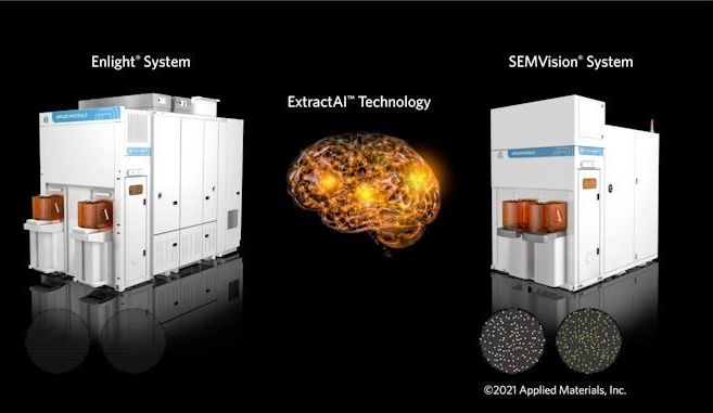
But finding and fixing defects is not easy today, as traditional optical inspection tools don’t offer sufficiently detailed image resolution, while high-resolution e-beam and multibeam inspection tools are relatively slow. Looking to bridge the gap on inspection costs and time, Applied Materials has been developing a technology called ExtractAI technology, which uses a combination of the company’s latest Enlight optical inspection tool, SEMVision G7 e-beam review system, and deep learning (AI) to quickly find flaws. And surprisingly, this solution has been in use for about a year now.
“Applied’s new playbook for process control combines Big Data and AI to deliver an intelligent and adaptive solution that accelerates our customers’ time to maximum yield,” said Keith Wells, group vice president and general manager, Imaging and Process Control at Applied Materials. “By combining our best-in-class optical inspection and eBeam review technologies, we have created the industry’s only solution with the intelligence to not only detect and classify yield-critical defects but also learn and adapt to process changes in real-time. This unique capability enables chipmakers to ramp new process nodes faster and maintain high capture rates of yield-critical defects over the lifetime of the process.”