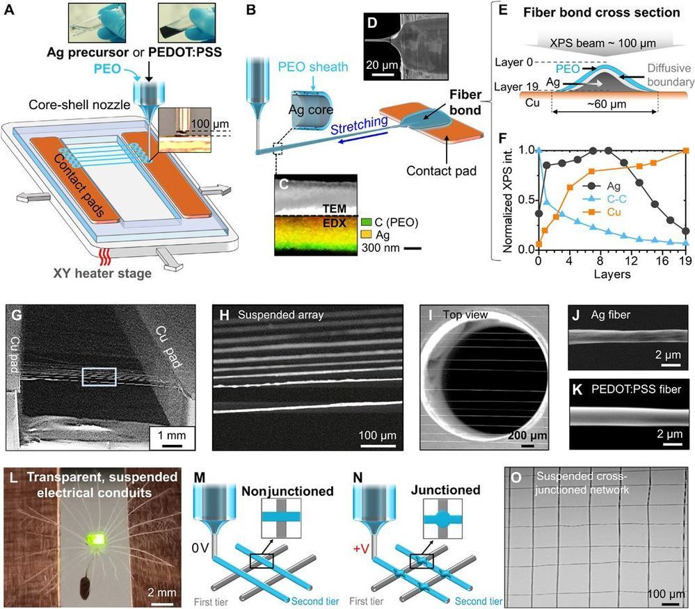
Scalability and device integration have been prevailing issues limiting our ability in harnessing the potential of small-diameter conducting fibers. We report inflight fiber printing (iFP), a one-step process that integrates conducting fiber production and fiber-to-circuit connection. Inorganic (silver) or organic {PEDOT: PSS [poly(3,4-ethylenedioxythiophene) polystyrene sulfonate]} fibers with 1- to 3-μm diameters are fabricated, with the fiber arrays exhibiting more than 95% transmittance (350 to 750 nm). The high surface area–to–volume ratio, permissiveness, and transparency of the fiber arrays were exploited to construct sensing and optoelectronic architectures. We show the PEDOT: PSS fibers as a cell-interfaced impedimetric sensor, a three-dimensional (3D) moisture flow sensor, and noncontact, wearable/portable respiratory sensors. The capability to design suspended fibers, networks of homo cross-junctions and hetero cross-junctions, and coupling iFP fibers with 3D-printed parts paves the way to additive manufacturing of fiber-based 3D devices with multilatitude functions and superior spatiotemporal resolution, beyond conventional film-based device architectures.
Small-diameter conducting fibers have unique morphological, mechanical, and optical properties such as high aspect ratio, low bending stiffness, directionality, and transparency that set them apart from other classes of conducting, film-based micro/nano structures (1–3). Orderly assembling of thin conducting fibers into an array or three-dimensional (3D) structures upscales their functional performance for device coupling. Developing new strategies to control rapid synthesis, patterning, and integration of these conducting elements into a device architecture could mark an important step in enabling new device functions and electronic designs (4, 5). To date, conducting micro/nanoscaled fibers have been produced and assembled in a number of ways, from transferring of chemically grown nanofibers/wires (6, 7), writing electrohydrodynamically deposited lines (8, 9), to drawing ultralong fibers (10, 11), wet spinning of fibers (12–14), and 2D/3D direct printing (15–18).