Scientists have managed to draw at high resolution and speed, local patterns in organic semiconductor films used in optoelectronic and photonic applications. The new method enables the patterning of material characteristics and concomitant final properties, including molecular conformation, orientation, crystallinity and composition. The technique, published with open access in Nature Communications, has also been patented and industrial partners are sought for further co-development.
Bridging the gap between organic electronics and the worldwide deployed silicon electronics requires new low cost and low energy consumption fabrication methods and technologies. This work represents a key enabling technology to accelerate the use of flexible and light-weight organic electronics and photonics to the level of silicon-based devices.
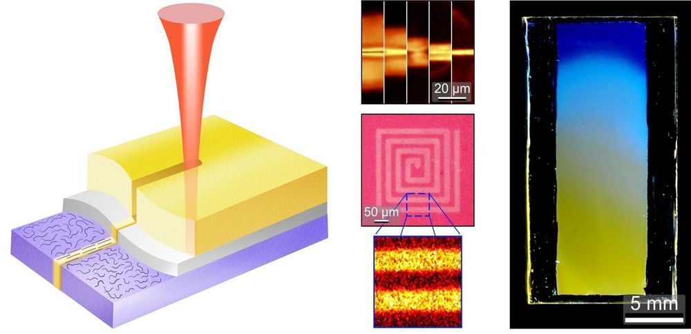
The microstructure and composition of organic semiconductors need to be tuned locally in order to optimize their properties, such as charge carrier mobility, electrical conductivity and light emission; and expand their functionalities for the practical upscaling of applications such as organic transistors (OFETs) and light emitting diodes (OLEDs), organic photovoltaics (OPV), organic thermoelectric generators (OTEGs), and organic photonic structures.