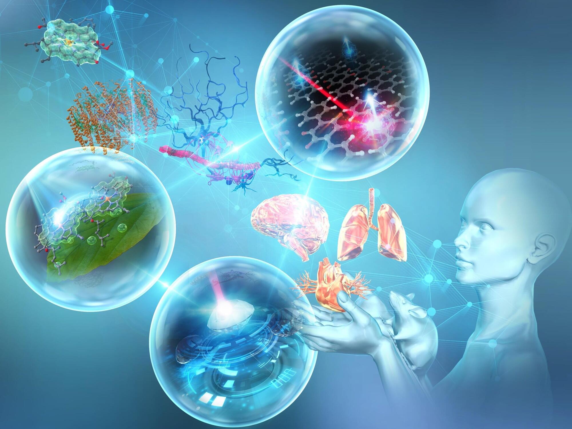
A team at Japan’s National Institutes for Quantum Science and Technology (QST) has published a field-defining Perspective that places the societal payoff of quantum technologies front and center: earlier disease detection, faster drug development, and new routes to clean energy. Their paper has been published online in the journal ACS Nano on December 18, 2025.
Get the latest international news and world events from around the world.
Two harmful gene variants can restore function when combined, study reveals
Sometimes, in genetics, two wrongs do make a right. A research team has recently shown that two harmful genetic variants, when occurring together in a gene, can restore function—proving a decades-old hypothesis originally proposed by Nobel laureate Francis Crick.
Their study, to be published in the Proceedings of the National Academy of Sciences, not only experimentally validated this theory but also introduced a powerful artificial intelligence (AI)-driven approach to genetic interpretation led by George Mason University researchers.
The project began when Aimée Dudley, a geneticist at the Pacific Northwest Research Institute (PNRI), approached George Mason University Chief AI Officer Amarda Shehu after following her lab’s work on frontier AI models for predicting the functional impact of genetic variation. That conversation sparked a collaboration that married PNRI’s experimental expertise with George Mason’s computational innovation to discover some surprising ways variant combinations can shape human health.
Human heart regrows muscle cells after heart attack, researchers discover
Pioneering research by experts at the University of Sydney, the Baird Institute and the Royal Prince Alfred Hospital in Sydney has shown that heart muscle cells regrow after a heart attack, opening up the possibility of new regenerative treatments for cardiovascular disease.
Following the publication of the study in Circulation Research, first author Dr. Robert Hume, from the Faculty of Medicine and Health and Charles Perkins Center, and Lead of Translational Research at the Baird Institute for Applied Heart and Lung Research, explained the significance of the finding: Until now we’ve thought that, because heart cells die after a heart attack, those areas of the heart were irreparably damaged, leaving the heart less able to pump blood to the body’s organs.
Our research shows that while the heart is left scarred after a heart attack, it produces new muscle cells, which opens up new possibilities.

Diabetes drugs may be changing cancer in surprising ways
Common diabetes drugs may do more than regulate blood sugar—they could also influence how cancers grow, spread, or slow down. Researchers are now unraveling how these medications affect immune function, inflammation, and tumor biology, with intriguing but still uncertain implications.
Researchers are taking a closer look at how medications used to treat diabetes may also influence cancer. While diabetes itself has long been associated with higher cancer risk, scientists are now investigating whether diabetes drugs play a direct role beyond controlling blood sugar levels and body weight. A recent review examines how widely used treatments such as metformin, SGLT2 inhibitors, and GLP-1 receptor agonists may affect cancer growth by changing how cells multiply, how the immune system responds, and how inflammation develops. These insights point to possible new treatment strategies while also highlighting how much remains unknown.
Type 2 Diabetes (T2DM) has been linked to a higher likelihood of developing several types of cancer, including liver, colorectal, and breast cancer. Managing blood glucose and body weight remains essential for people with diabetes, but growing evidence suggests these factors alone do not fully explain the increased cancer risk. This has led scientists to explore how diabetes medications themselves might influence cancer, either by reducing risk or, in some cases, creating unintended effects. Understanding this connection could help clarify how diabetes treatments fit into cancer prevention and care, though further research is still needed to unravel the underlying biology.
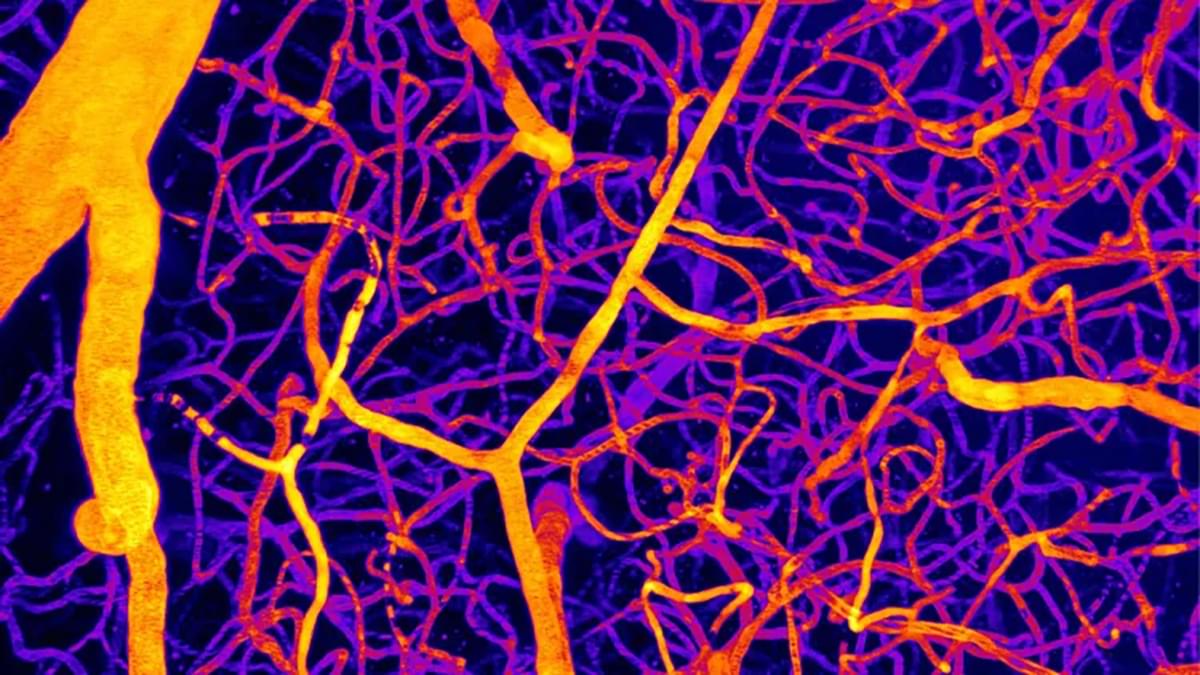
A Single Molecule May Explain How Blood Flow in The Brain Triggers Dementia
Reduced blood flow to the brain is thought to be a key factor in many forms of dementia, including Alzheimer’s, and scientists have just identified a new mechanism regulating this flow, which may also help explain how it goes wrong.
A fat molecule helps maintain the system’s balance, researchers at the University of Vermont discovered, and in mouse models of Alzheimer’s disease, disruption of this balance led to problems.
Fixing the imbalance restored more normal blood flow, offering a hopeful new target for understanding and treating dementia-related brain changes.
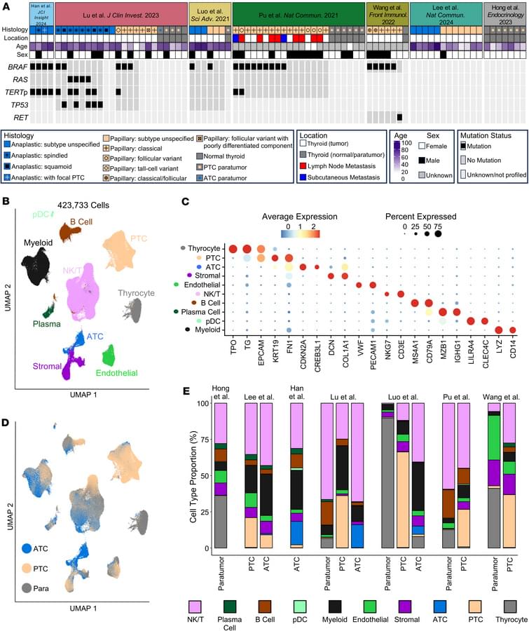
Presenting data from the largest integrated thyroid cancer single-cell sequencing atlas
Here, Vivian L. Weiss & team highlight stromal tumor-dynamics occurring across the spatial evolution of thyroid cancer from indolent to lethal disease, identifying a prognostic invasive cell subtype:
The figure shows two distinct patterns associated with anaplastic thyroid carcinoma.
6The Francis Crick Institute, London, United Kingdom.
7Institute of Interdisciplinary Research (IRIBHM), Universite Libre de Bruxelles, Brussels, Belgium.
8Department of Laboratory Medicine and Pathology, University of Washington School of Medicine, Seattle, Washington, USA.
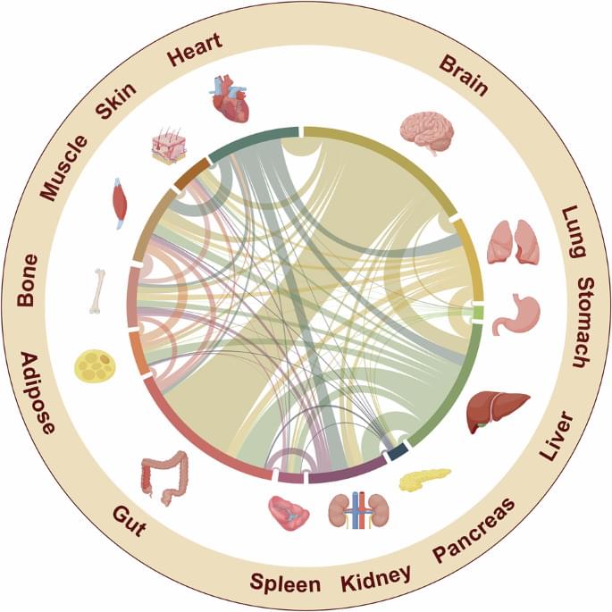
Organ cross-talk: molecular mechanisms, biological functions, and therapeutic interventions for diseases
3. Pathology as Network Dysregulation.
In recent years, a transformative view of physiology has emerged: the body operates not as isolated organs, but as an integrated communication network in which signals flow bidirectionally between the brain, the immune system, the gut, and peripheral organs. This comprehensive review synthesizes current mechanistic insights into this “organ cross-talk” and frames them within systems biology and neuroscience.
At its core, organ cross-talk encompasses neural, endocrine, metabolic, and immune signaling between organs that coordinate homeostasis and orchestrate responses to stress and disease. From a neuroscience vantage point, three themes stand out:
1. The Brain as a Communication Hub.
2. Peripheral Feedback to the CNS.

First Dawn of Universe Simulation: EWOG
From Dark till First Dawn of Universe Simulation: EWOG Quantum Gravity Theory.
🚀From Dark till First Dawn of Universe Simulation: Why EWOG is promising to the Cosmic Race! 🌌 https://lnkd.in/gFBNsKtq Ever wonder how the James Webb Space Telescope (JWST) keeps finding massive, mature galaxies that “shouldn’t exist” yet? Standard cosmology (ΛCDM) is struggling to explain this without extreme fine-tuning. But Entanglement-Weighted Operator Gravity (EWOG) provides a first-principles answer. 🧩 The “Quantum Turbo” Effect In the dense early universe, high quantum entanglement between matter and geometry temporarily boosted gravity’s strength. The Core Idea: Gravity isn’t a constant; it’s an operator weighted by entanglement (Ŵ). * Curvature from Commutators: R̂ᵤᵥ = [∇̂ᵤ, ∇̂ᵥ] * The Boosted Coupling: G_eff(a, k) = G_N [1 + α₀(1 — e⁻ᵐʳ)ℱ] This “turbo boost” allowed gas to collapse into stars 150,000 years earlier than standard models predict.

Agenus Closes Strategic Immunotherapeutic Collaboration with Zydus Lifesciences
As part of the collaboration, Agenus has granted Zydus exclusive rights to develop and commercialize BOT and BAL in India and Sri Lanka, with Agenus eligible to receive royalties on net sales in those territories.
“Closing this collaboration with Zydus strengthens our balance sheet and, critically, secures dedicated U.S. manufacturing capacity at a pivotal moment for Agenus,” continued Armen. “With these foundations in place, our focus in 2026 is disciplined execution—advancing our Phase III program, broadening paid patient access through authorized pathways, and progressing toward regulatory submission supported by one of the most substantial clinical datasets generated in [microsatellite stable] MSS colorectal cancer.”
Following the closing, the Emeryville and Berkeley, CA, biologics manufacturing facilities will be transferred to Zydus and housed under a newly formed subsidiary named Zylidac Bio. Agenus has secured committed manufacturing capacity at these U.S. sites to support BOT+BAL supply needs for its clinical trials, global access programs, and future commercialization.
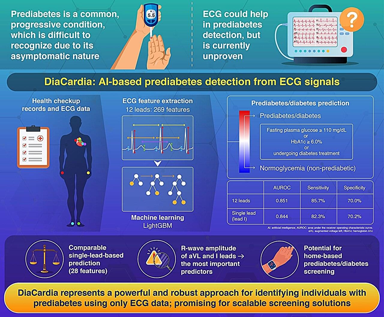
AI model detects prediabetes using ECG data without need for blood tests
DiaCardia, a novel artificial intelligence model that can accurately identify individuals with prediabetes using either 12-lead or single-lead electrocardiogram (ECG) data, has been developed. This breakthrough holds promise for future home-based prediabetes screening using consumer wearable devices, without requiring invasive blood tests.
Type 2 diabetes occurs when the human body either cannot make enough insulin or does not use insulin well, resulting in high blood glucose levels. This condition is a growing global health burden that can reduce the quality of life and life expectancy.
Before type 2 diabetes develops, many people go through a prolonged stage called prediabetes, where blood glucose levels are above normal but not high enough to be diagnosed as diabetes. Prediabetes is an important window wherein lifestyle changes can reduce the progression to diabetes.