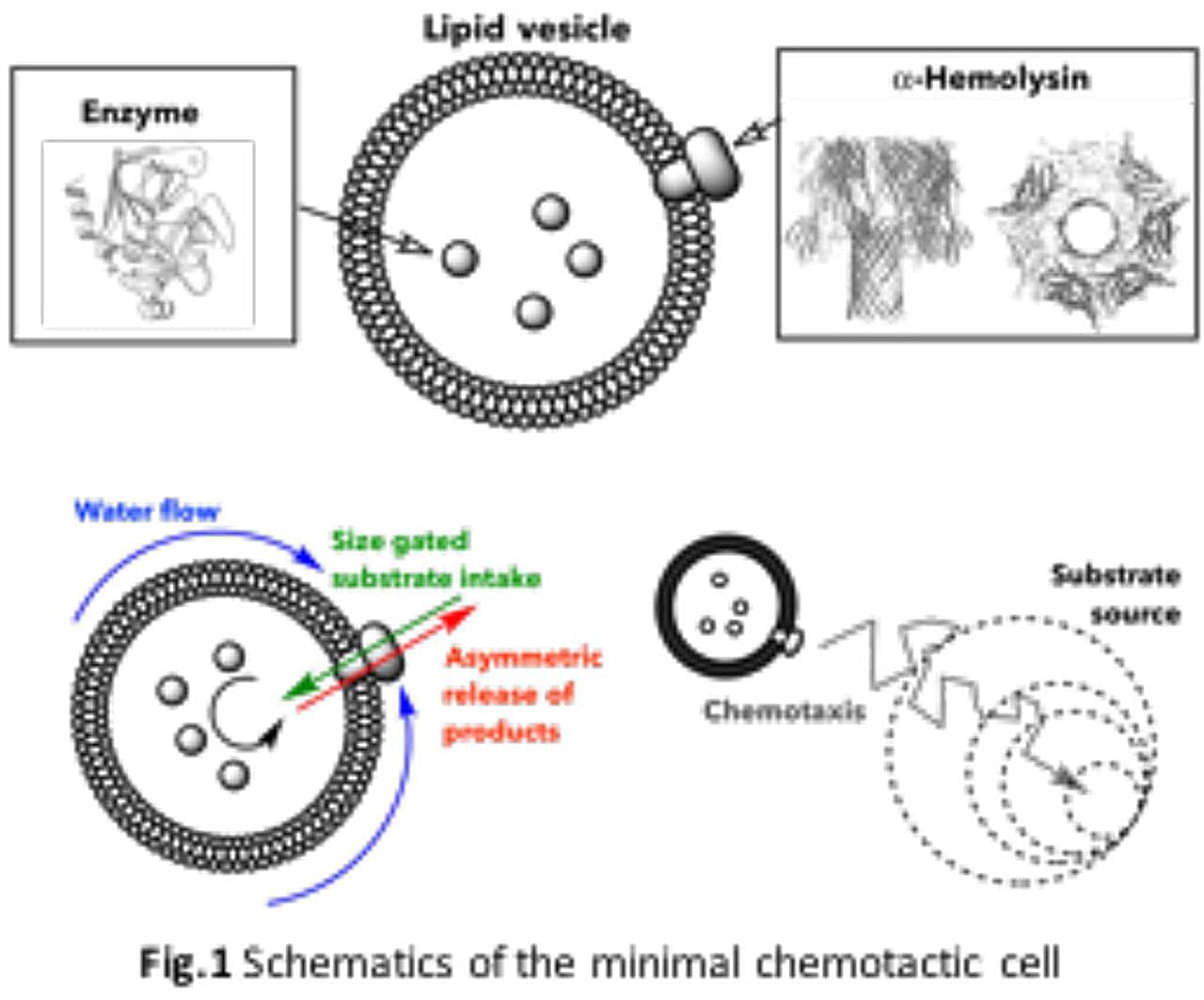
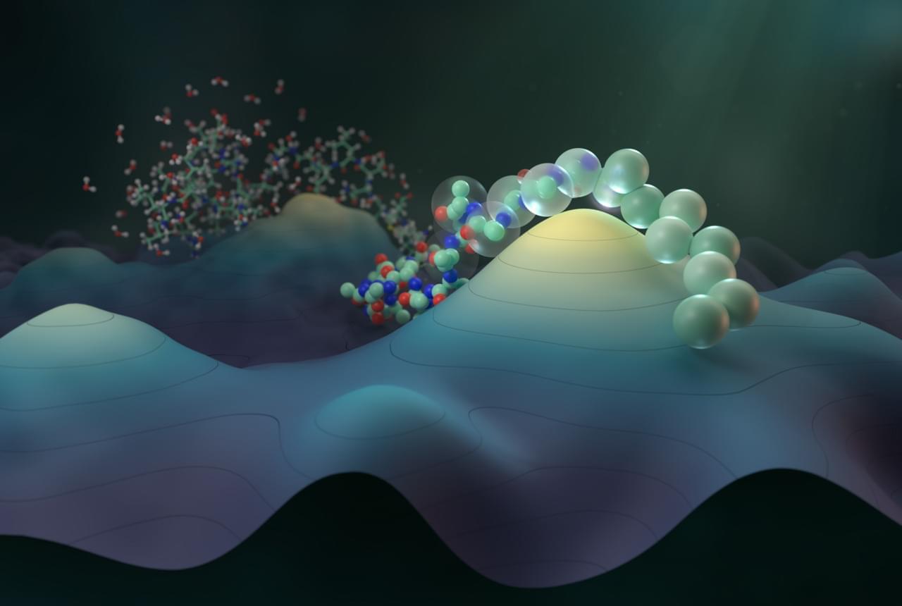
Researchers at the Institute for Bioengineering of Catalonia (IBEC) have created the world’s simplest artificial cell capable of chemical navigation, migrating toward specific substances like living cells do.
This breakthrough, published in Science Advances, demonstrates how microscopic bubbles can be programmed to follow chemical trails. The study describes the development of a “minimal cell” in the form of a lipid vesicle encapsulating enzymes that can propel itself through chemotaxis.
Cellular transport is a vital aspect of many biological processes and a key milestone in evolution. Among all types of movement, chemotaxis is an essential strategy used by many living systems to move towards beneficial signals, such as nutrients, or away from harmful ones.

