NIH-funded research finds evidence of antibiotic-resistant gut bacteria.
This would help understand the artificial neural networks or ANN which are AI models and programs that mimic the working of the human brain so that machines can learn to make decisions in a more human-like manner.
Jeff Dahn works with Tesla alongside his individual research pursuits. He’s discovered a chemistry that might make robo-taxis and longer-range EVs a reality.
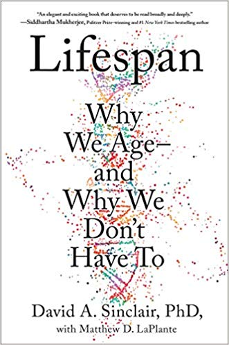
Lifespan: Why We Age-and Why We Don’t Have To — Kindle edition by David A. Sinclair, Matthew D. LaPlante. Download it once and read it on your Kindle device, PC, phones or tablets. Use features like bookmarks, note taking and highlighting while reading Lifespan: Why We Age-and Why We Don’t Have To.
Researchers at the University of California, Los Angeles (UCLA) and the California NanoSystems Institute in Los Angeles have recently developed a soft swimming robot based on a self-sustained hydrogel oscillator. This robot, presented in a paper published in Science Robotics, operates under constant light input without the need for a battery.
“When I shone light on a soft, fast responsive hydrogel pillar, I observed the pillar started to oscillate around the optical beam,” Yusen Zhao, a Ph.D. student involved in the research, said. “It looked very intriguing to me, and I wondered: How can a constant input produce intermittent output? Under what conditions does the oscillation happen? Would it be powerful enough to propel and swim in water, and eventually lead to solar sails? With these questions, I continued systematic studies aiming to achieve these objectives.”
Zhao and his colleagues developed a soft oscillator made of a light-responsive soft gel, which is molded into the shape of a pillar or strip. When light hits a spot of this gel pillar, it is automatically absorbed and converted into heat. The locally heated spot on the robot causes it to eject some of its water and shrink in volume, resulting in its tail bending towards the light source.
(TT) — Thanks to the ingenuity of a blind inventor, people who lack sight can more easily navigate the world.
Cupertino calling. Join us for an Apple special event live from the Steve Jobs Theater on September 10 at 10 a.m. PDT. Set a reminder and we’ll send an update before the show.
Revolutionary research is underway to create a cheap, fast, at-home early diagnostic test.
Researchers at Mayo Clinic have identified the enzyme, called CD38, that is responsible for the decrease in nicotinamide adenine dinucleotide (NAD) during aging, a process that is associated with age-related metabolic decline. Results demonstrated an increase in the presence of CD38 with aging in both mice and humans. The results appear today in Cell Metabolism.
“As we age, we experience a decline in our metabolism and metabolic function. This increases the incidence of age-related metabolic diseases like obesity, diabetes and others,” says Eduardo Chini, M.D., Ph.D., anesthesiologist and researcher for Mayo Clinic’s Robert and Arlene Kogod Center on Aging and lead author of the study. “Previous studies have shown that levels of NAD decline during the aging process in several organisms. This decrease in NAD appears to be, at least in part, responsible for age-related metabolic decline.”
In this study, researchers at the Center on Aging have shown that CD38, an enzyme that is present in inflammatory cells, is directly involved in the process that mediates the age-related NAD decline. Comparing 3- to 32-month-old mice, researchers found that levels of CD38 increased at least two to three times during chronological aging in all tissues tested, including the liver, fat, spleen and skeletal muscle.


