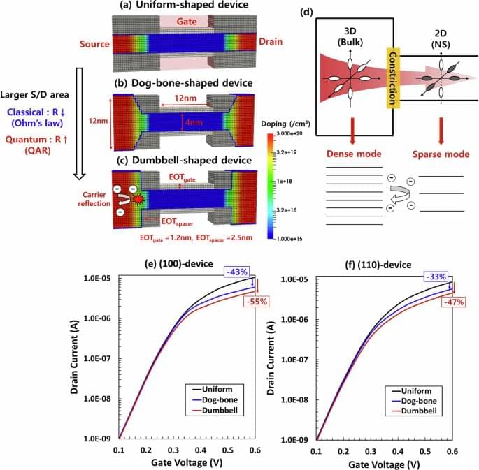
In nanoscale transistors, quantum mechanical effects such as tunneling and quantization significantly influence device characteristics. However, large-scale quantum transport simulation remains a challenging field, making it difficult to account for quantum mechanical effects arising from the complex device geometries. Here, based on large-scale quantum transport simulations, we demonstrate that quantum geometrical effects in stacked nanosheet GAAFETs significantly impact carrier injection characteristics. Discontinuities in confinement energy at the constriction—the junction between the bulk source/drain and nanosheet channel—cause substantial carrier backscattering. This degradation becomes more severe as electrons experience higher effective energy barriers, and is further exacerbated at lower scattering rate, lower doping concentrations, and near Schottky barriers where electron depletion regions form. Considering these quantum mechanical bottlenecks, proper device optimization for future technology nodes requires a full quantum-based device structure design at the large-scale level, which enables unique optimization strategies beyond conventional classical prediction.
Kyoung Yeon Kim and colleagues report the importance of quantum geometrical effects that serve as a bottleneck in stacked nanosheet GAAFETs. This highlights that full quantum mechanics-based device design is crucial for realizing ideal carrier injection characteristics in future technology nodes.

